Three-in-one 2D perovskite functional gated organic thin-film transistors: Integrated sensing, memory and computing
IF 9.7
2区 材料科学
Q1 MATERIALS SCIENCE, MULTIDISCIPLINARY
引用次数: 0
Abstract
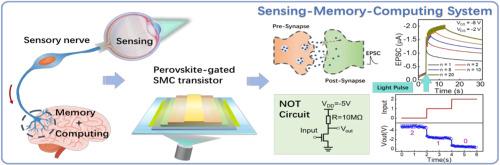
Sensing-memory-computing (SMC) technology, that integrates the information perception, memory and processing functions in one physical unit, has promised an innovative architecture for future machine vision system with extreme energy and time efficiency by fundamentally eliminating the interfaces between the separation units in the current systems. To achieve this goal, it is required to develop novel device structure for integrating multiple functional attributes. This study presents an innovative organic thin-film transistor (OTFT) based on a two-dimensional (2D) perovskite as functional gate dielectric, that integrates the photodetection, memory, and computing in one unit by synergistically exploiting the effects of ion migration, optoelectronic property, and photo-generated charge trapping. The OTFTs exhibit excellent nonvolatile memory (NVM) properties, with the low programming/erasing (P/E) voltages of ±10 V, ultrafast P/E ability of 5 ms, highly stable retention and reliable endurance. The three-in-one OTFTs also demonstrate: (1) real-time physiological signal monitoring through optical sensing, (2) binary reconfigurable (AND and OR) logic-in-memory circuits and ternary operations (NOT, NAND, and NOR) in the logic-in-memory circuits, (3) emulation of optoelectronic synaptic plasticity. Furthermore, the OTFTs array effectively perceives and stores patterns of “J”, “L”, and “U” letters with retina-like functionality. Our work establishes a promising paradigm for developing high-performance, energy-efficient SMC hardware for next-generation artificial intelligent applications.

三合一二维钙钛矿功能门控有机薄膜晶体管:集成传感、存储和计算
传感记忆计算(SMC)技术将信息感知、记忆和处理功能集成在一个物理单元中,从根本上消除了当前系统中分离单元之间的接口,为未来的机器视觉系统提供了一种创新的架构,具有极高的能量和时间效率。为了实现这一目标,需要开发集成多种功能属性的新型器件结构。本研究提出了一种基于二维(2D)钙钛矿作为功能栅极电介质的创新有机薄膜晶体管(OTFT),通过协同利用离子迁移、光电特性和光产生的电荷捕获的影响,将光探测、存储和计算集成在一个单元中。OTFTs具有优异的非易失性存储器(NVM)性能,具有±10 V的低编程/擦除(P/E)电压,5 ms的超快P/E能力,高度稳定的保留和可靠的耐用性。三合一OTFTs还展示了:(1)通过光传感实时监测生理信号;(2)二进制可重构(AND和OR)逻辑存储电路和逻辑存储电路中的三元运算(NOT, NAND和NOR);(3)光电突触可塑性仿真。此外,OTFTs阵列具有类似视网膜的功能,可以有效地感知和存储“J”、“L”和“U”字母的模式。我们的工作为下一代人工智能应用开发高性能,节能的SMC硬件建立了一个有前途的范例。
本文章由计算机程序翻译,如有差异,请以英文原文为准。
求助全文
约1分钟内获得全文
求助全文
来源期刊
Materials Today Physics
Materials Science-General Materials Science
CiteScore
14.00
自引率
7.80%
发文量
284
审稿时长
15 days
期刊介绍:
Materials Today Physics is a multi-disciplinary journal focused on the physics of materials, encompassing both the physical properties and materials synthesis. Operating at the interface of physics and materials science, this journal covers one of the largest and most dynamic fields within physical science. The forefront research in materials physics is driving advancements in new materials, uncovering new physics, and fostering novel applications at an unprecedented pace.
 求助内容:
求助内容: 应助结果提醒方式:


