Haichuan Li, Yongyu Wu, Dawei Gao, Kai Xu, Kun Ren, Dianyu Qi
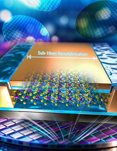
{"title":"Recent Progress in Sub-10 Nm Nanofabrication for Scaling Down 2D Transistors","authors":"Haichuan Li, Yongyu Wu, Dawei Gao, Kai Xu, Kun Ren, Dianyu Qi","doi":"10.1002/aelm.202500306","DOIUrl":null,"url":null,"abstract":"<p>2D field-effect transistors (2D-FETs) leverage atomically thin, dangling-bond-free channels to overcome short-channel effects and surface defects in sub-10 nm nodes. However, conventional lithography hardly meets the requirement of sub-10 nm nanofabrication because of resolution limits, making the fabrication of 2D-FETs with sub-10 nm channel lengths still a significant challenge. Here, strategies of realizing 2D-FETs are reviewed with sub-10 nm channels: i) Ultraprecise nanolithography, including electron-beam lithography, cold development, and block copolymers (BCP)-based directed self-assembly (DSA); ii) Nanogap formation, leveraging stress-induced cracking, grain-boundary widening, electromigration, carbon-nanotube masking, and shadow evaporation; iii) Vertical-channel architectures, where channel length is defined by dielectric thickness in metal–insulator–metal stacks or barristor structures; iv) Self-aligned isolation, employing ultrathin film oxidation, adhesion lithography, and heterostructure undercut processes to precisely define source-drain separations. Key performance metrics are compiled and compared—contact resistance, on-state current, off-state leakage, DIBL, and subthreshold swing—across representative devices, illustrating the robust scaling immunity of 2D materials. Finally, emerging “lab-to-fab” approaches are discussed, such as edge lithography, mechanical cracking, and post-pattern modification, pointing toward scalable, low-cost manufacturing of wafer-scale sub-10 nm 2D-FETs. This outlook provides practical guidelines for future integrated circuit implementations based on 2D semiconductors.</p>","PeriodicalId":110,"journal":{"name":"Advanced Electronic Materials","volume":"11 16","pages":""},"PeriodicalIF":5.3000,"publicationDate":"2025-09-24","publicationTypes":"Journal Article","fieldsOfStudy":null,"isOpenAccess":false,"openAccessPdf":"https://advanced.onlinelibrary.wiley.com/doi/epdf/10.1002/aelm.202500306","citationCount":"0","resultStr":null,"platform":"Semanticscholar","paperid":null,"PeriodicalName":"Advanced Electronic Materials","FirstCategoryId":"88","ListUrlMain":"https://advanced.onlinelibrary.wiley.com/doi/10.1002/aelm.202500306","RegionNum":2,"RegionCategory":"材料科学","ArticlePicture":[],"TitleCN":null,"AbstractTextCN":null,"PMCID":null,"EPubDate":"","PubModel":"","JCR":"Q2","JCRName":"MATERIALS SCIENCE, MULTIDISCIPLINARY","Score":null,"Total":0}
引用次数: 0
Abstract
2D field-effect transistors (2D-FETs) leverage atomically thin, dangling-bond-free channels to overcome short-channel effects and surface defects in sub-10 nm nodes. However, conventional lithography hardly meets the requirement of sub-10 nm nanofabrication because of resolution limits, making the fabrication of 2D-FETs with sub-10 nm channel lengths still a significant challenge. Here, strategies of realizing 2D-FETs are reviewed with sub-10 nm channels: i) Ultraprecise nanolithography, including electron-beam lithography, cold development, and block copolymers (BCP)-based directed self-assembly (DSA); ii) Nanogap formation, leveraging stress-induced cracking, grain-boundary widening, electromigration, carbon-nanotube masking, and shadow evaporation; iii) Vertical-channel architectures, where channel length is defined by dielectric thickness in metal–insulator–metal stacks or barristor structures; iv) Self-aligned isolation, employing ultrathin film oxidation, adhesion lithography, and heterostructure undercut processes to precisely define source-drain separations. Key performance metrics are compiled and compared—contact resistance, on-state current, off-state leakage, DIBL, and subthreshold swing—across representative devices, illustrating the robust scaling immunity of 2D materials. Finally, emerging “lab-to-fab” approaches are discussed, such as edge lithography, mechanical cracking, and post-pattern modification, pointing toward scalable, low-cost manufacturing of wafer-scale sub-10 nm 2D-FETs. This outlook provides practical guidelines for future integrated circuit implementations based on 2D semiconductors.
期刊介绍:
Advanced Electronic Materials is an interdisciplinary forum for peer-reviewed, high-quality, high-impact research in the fields of materials science, physics, and engineering of electronic and magnetic materials. It includes research on physics and physical properties of electronic and magnetic materials, spintronics, electronics, device physics and engineering, micro- and nano-electromechanical systems, and organic electronics, in addition to fundamental research.


 求助内容:
求助内容: 应助结果提醒方式:


