Electron beam surface patterning of Se alloys
IF 4.6
3区 工程技术
Q2 ENGINEERING, ELECTRICAL & ELECTRONIC
引用次数: 0
Abstract
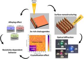
Amorphous chalcogen alloys based on selenium (Se) and tellurium (Te) are extensively studied due to their unique physical properties. These materials find practical applications in infrared technologies, micro- and nano-electronics, nano-optics, photonics, and optoelectronics. Recently, laser and electron beam irradiations were shown to lead to surface mass transport or local density variations on Se-based amorphous alloys, and thus, to allow the surfaces of these chalcogen alloys to be patterned without the use of a mask such as for conventional lithography. The driving force of this phenomenon is assumed to be linked to charge accumulation in the irradiated regions, causing significant repulsion between ions in the film, leading to the local modification of the film volume or to mass transport in the vicinity of the film surface. In this work, room-temperature electron beam structuring effect is investigated on both amorphous and crystalline Se-rich chalcogen alloy thin films, exploring the potential of this technique for large-scale chalcogen alloy surface patterning, and providing new insights on the mechanism driving chalcogen alloy structuring by electron beam irradiations.
Se合金的电子束表面图案化
基于硒(Se)和碲(Te)的非晶态硫合金因其独特的物理性能而受到广泛的研究。这些材料在红外技术、微纳米电子学、纳米光学、光子学和光电子学中有实际应用。最近,激光和电子束辐照被证明会导致se基非晶合金的表面质量输运或局部密度变化,因此,可以在不使用掩模(如传统光刻)的情况下对这些硫合金表面进行图像化。这种现象的驱动力被认为与受辐照区域的电荷积累有关,引起膜中离子之间的明显排斥,导致膜体积的局部改变或膜表面附近的质量输运。本文研究了非晶型和结晶型富硒硫合金薄膜的室温电子束结构效应,探索了该技术在大规模富硒硫合金表面图像化方面的潜力,并为电子束辐照驱动富硒硫合金结构的机理提供了新的见解。
本文章由计算机程序翻译,如有差异,请以英文原文为准。
求助全文
约1分钟内获得全文
求助全文
来源期刊

Materials Science in Semiconductor Processing
工程技术-材料科学:综合
CiteScore
8.00
自引率
4.90%
发文量
780
审稿时长
42 days
期刊介绍:
Materials Science in Semiconductor Processing provides a unique forum for the discussion of novel processing, applications and theoretical studies of functional materials and devices for (opto)electronics, sensors, detectors, biotechnology and green energy.
Each issue will aim to provide a snapshot of current insights, new achievements, breakthroughs and future trends in such diverse fields as microelectronics, energy conversion and storage, communications, biotechnology, (photo)catalysis, nano- and thin-film technology, hybrid and composite materials, chemical processing, vapor-phase deposition, device fabrication, and modelling, which are the backbone of advanced semiconductor processing and applications.
Coverage will include: advanced lithography for submicron devices; etching and related topics; ion implantation; damage evolution and related issues; plasma and thermal CVD; rapid thermal processing; advanced metallization and interconnect schemes; thin dielectric layers, oxidation; sol-gel processing; chemical bath and (electro)chemical deposition; compound semiconductor processing; new non-oxide materials and their applications; (macro)molecular and hybrid materials; molecular dynamics, ab-initio methods, Monte Carlo, etc.; new materials and processes for discrete and integrated circuits; magnetic materials and spintronics; heterostructures and quantum devices; engineering of the electrical and optical properties of semiconductors; crystal growth mechanisms; reliability, defect density, intrinsic impurities and defects.
 求助内容:
求助内容: 应助结果提醒方式:


