Hydrogen gas sensing enhancement with gamma-irradiated S-CNT/V2O5 thin film: A synergistic effect
IF 4.6
3区 工程技术
Q2 ENGINEERING, ELECTRICAL & ELECTRONIC
引用次数: 0
Abstract
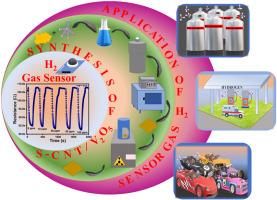
The present study intends to examine the effect of gamma irradiation on single-wall carbon nanotube-dopedvanadium pentoxide (S-CNT/V2O5) thin films. This was accomplished by synthesizing S-CNT/V2O5 nanoparticles using a hydrothermal route and fabricating them into thin films using the spin-coating technique. The as-synthesized thin films were irradiated with gamma rays at different doses, viz. 0.1, 10, and 50 kGy. The X-ray diffraction revealed that the film showed an orthorhombic structure, and with increasing the gamma dose, the crystallite size and the optical band gap as obtained by using UV–vis spectroscopy decreased from 55.68 to 49.69 nm and 3.15 to 2.82 eV, respectively. The other characterizations like field emission electron scanning microscopy (FE-SEM), energy dispersive analysis of X-ray (EDAX), and X-Ray Photoelectron Spectroscopy (XPS) were also performed to study the surface and elemental composition of thin films. The gas-sensing characteristics of these thin films-cum-sensors were determined by exposing them with different concentrations of H2 gas ranging from 5 ppm to 100 ppm. The sensor irradiated with 50 kGy dose of gamma photons showed enhanced sensitivity of 140 % for 100 ppm H2 gas concentration with response and recovery times of 42.4 and 78.3 s, respectively, at 100 °C. The selectivity of the sensor was tested using the reducing and oxidising gases of CO, NO2, NH3 and H2 at 100 °C for 100 ppm gas concentration. Among these gases, the sensor showed the best sensing response towards H2 gas. The performance of the sensor after 90 days remained satisfactory.
γ辐照S-CNT/V2O5薄膜增强氢气传感:协同效应
本研究旨在研究伽马辐照对单壁碳纳米管掺杂五氧化二钒(S-CNT/V2O5)薄膜的影响。这是通过水热方法合成S-CNT/V2O5纳米颗粒,并使用自旋涂层技术将其制成薄膜来实现的。用不同剂量(0.1、10和50 kGy)的伽马射线照射合成的薄膜。x射线衍射结果表明,薄膜呈正交结构,随着γ剂量的增加,晶体尺寸和带隙分别从55.68 nm减小到49.69 nm和3.15 eV减小到2.82 eV。利用场发射电子扫描显微镜(FE-SEM)、x射线能量色散分析(EDAX)和x射线光电子能谱(XPS)等表征手段研究了薄膜的表面和元素组成。通过将这些薄膜-传感器暴露在不同浓度的H2气体中(从5 ppm到100 ppm),确定了这些薄膜-传感器的气敏特性。在100°C条件下,用50 kGy剂量的伽玛光子辐照后,传感器在氢气浓度为100 ppm时的灵敏度提高了140%,响应时间和恢复时间分别为42.4 s和78.3 s。在100℃、100 ppm气体浓度下,用CO、NO2、NH3和H2等还原性和氧化性气体对传感器的选择性进行了测试。其中,传感器对H2气体的传感响应最好。90天后,传感器的性能仍然令人满意。
本文章由计算机程序翻译,如有差异,请以英文原文为准。
求助全文
约1分钟内获得全文
求助全文
来源期刊

Materials Science in Semiconductor Processing
工程技术-材料科学:综合
CiteScore
8.00
自引率
4.90%
发文量
780
审稿时长
42 days
期刊介绍:
Materials Science in Semiconductor Processing provides a unique forum for the discussion of novel processing, applications and theoretical studies of functional materials and devices for (opto)electronics, sensors, detectors, biotechnology and green energy.
Each issue will aim to provide a snapshot of current insights, new achievements, breakthroughs and future trends in such diverse fields as microelectronics, energy conversion and storage, communications, biotechnology, (photo)catalysis, nano- and thin-film technology, hybrid and composite materials, chemical processing, vapor-phase deposition, device fabrication, and modelling, which are the backbone of advanced semiconductor processing and applications.
Coverage will include: advanced lithography for submicron devices; etching and related topics; ion implantation; damage evolution and related issues; plasma and thermal CVD; rapid thermal processing; advanced metallization and interconnect schemes; thin dielectric layers, oxidation; sol-gel processing; chemical bath and (electro)chemical deposition; compound semiconductor processing; new non-oxide materials and their applications; (macro)molecular and hybrid materials; molecular dynamics, ab-initio methods, Monte Carlo, etc.; new materials and processes for discrete and integrated circuits; magnetic materials and spintronics; heterostructures and quantum devices; engineering of the electrical and optical properties of semiconductors; crystal growth mechanisms; reliability, defect density, intrinsic impurities and defects.
 求助内容:
求助内容: 应助结果提醒方式:


