Supercritical fluid-mediated exfoliation of NbSe2 and fabrication of RGO-NbSe2 nanostructures for enhanced hydrogen evolution
IF 4.6
3区 工程技术
Q2 ENGINEERING, ELECTRICAL & ELECTRONIC
引用次数: 0
Abstract
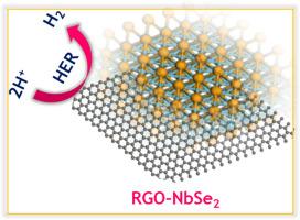
Uniform rod-like NbSe2 nanostructures were precisely fabricated from bulk NbSe2 using a one-pot, rapid supercritical fluid process, where a mildly basic solution acted as the exfoliating agent. The formation of NbSe2 nanorods was confirmed by microscopic analyses. XRD, Raman, and XPS results further validated the successful exfoliation and indicated partial surface oxidation of NbSe2 into Nb2O5 nanostructures during SCF processing. Interestingly, the formation of rod-like NbSe2 was largely suppressed in the synthesis of RGO-NbSe2 nanocomposites, as the RGO nanosheets hindered the growth of such morphologies. The synthesized RGO-NbSe2 nanocomposites exhibited outstanding electrocatalytic activity toward hydrogen evolution, requiring only ∼123 mV overpotential to reach 10 mA cm−2. This performance notably surpassed that of the pristine NbSe2 nanorods, which required ∼355 mV for the same current density. This enhancement is attributed to the efficient exfoliation of bulk NbSe2 into nanosheets, which enhances the exposure of reactive edge sites and promotes the formation of heterostructures with favourable hydrogen adsorption characteristics. The integration with highly conductive RGO further contributes to charge transfer and overall catalytic synergy.
超临界流体介导的NbSe2剥离及RGO-NbSe2纳米结构的制备
均匀的棒状NbSe2纳米结构是用一锅快速超临界流体工艺从块状NbSe2中精确制备的,其中温和的碱性溶液作为去死皮剂。显微分析证实了NbSe2纳米棒的形成。XRD、Raman和XPS结果进一步证实了SCF的成功剥离,并表明NbSe2在SCF加工过程中部分表面氧化成Nb2O5纳米结构。有趣的是,在RGO-NbSe2纳米复合材料的合成过程中,棒状NbSe2的形成在很大程度上受到抑制,因为RGO纳米片阻碍了这种形态的生长。合成的RGO-NbSe2纳米复合材料表现出优异的析氢电催化活性,仅需~ 123 mV过电位即可达到10 mA cm−2。这种性能明显超过了原始的NbSe2纳米棒,后者在相同的电流密度下需要~ 355 mV。这种增强归因于块状NbSe2有效地剥落成纳米片,这增加了活性边缘位点的暴露,促进了具有良好氢吸附特性的异质结构的形成。与高导电性RGO的整合进一步有助于电荷转移和整体催化协同作用。
本文章由计算机程序翻译,如有差异,请以英文原文为准。
求助全文
约1分钟内获得全文
求助全文
来源期刊

Materials Science in Semiconductor Processing
工程技术-材料科学:综合
CiteScore
8.00
自引率
4.90%
发文量
780
审稿时长
42 days
期刊介绍:
Materials Science in Semiconductor Processing provides a unique forum for the discussion of novel processing, applications and theoretical studies of functional materials and devices for (opto)electronics, sensors, detectors, biotechnology and green energy.
Each issue will aim to provide a snapshot of current insights, new achievements, breakthroughs and future trends in such diverse fields as microelectronics, energy conversion and storage, communications, biotechnology, (photo)catalysis, nano- and thin-film technology, hybrid and composite materials, chemical processing, vapor-phase deposition, device fabrication, and modelling, which are the backbone of advanced semiconductor processing and applications.
Coverage will include: advanced lithography for submicron devices; etching and related topics; ion implantation; damage evolution and related issues; plasma and thermal CVD; rapid thermal processing; advanced metallization and interconnect schemes; thin dielectric layers, oxidation; sol-gel processing; chemical bath and (electro)chemical deposition; compound semiconductor processing; new non-oxide materials and their applications; (macro)molecular and hybrid materials; molecular dynamics, ab-initio methods, Monte Carlo, etc.; new materials and processes for discrete and integrated circuits; magnetic materials and spintronics; heterostructures and quantum devices; engineering of the electrical and optical properties of semiconductors; crystal growth mechanisms; reliability, defect density, intrinsic impurities and defects.
 求助内容:
求助内容: 应助结果提醒方式:


