Resistless photomask fabrication using electrolithography
IF 3.1
Q2 ENGINEERING, ELECTRICAL & ELECTRONIC
引用次数: 0
Abstract
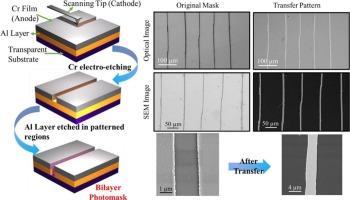
Photolithography is the most widely used lithography technique for commercial fabrication of micro-devices as well as for research and development purposes. However, to perform photolithography, we need a photomask containing the desired pattern. Conventional methods of photomask fabrication involve either photolithography using a direct laser writer or electron-beam lithography. Interestingly, the rise of sequential write scanning probe lithography (SPL) techniques has given rise to various novel methods of direct photomask writing. In this study, we focus on photomask fabrication using a SPL technique, known as ‘Electrolithography’ (ELG), with which multi-scale features can be easily patterned. This is a subtractive lithography technique that involves direct patterning on chromium (Cr) thin films. Being an electrical and direct-write process, ELG bypasses the need for high-power UV laser, electron gun, and polymer resist layers thereby making the process cost-effective and carbon-efficient. We propose a resistless, reliable and novel photomask fabrication process, using the ELG technique, based on a bimetallic architecture. Using the proposed method, we were able to obtain lines having a width of <2 μm, in the best case, and lines with a width < 10 μm repeatedly. We were also able to transfer the fabricated patterns reliably and repeatedly onto a material of choice.
利用电光刻技术制造无电阻光掩膜
光刻技术是微器件商业制造以及研究和开发中应用最广泛的光刻技术。然而,为了进行光刻,我们需要一个包含所需图案的掩模。传统的掩模制造方法包括使用直接激光书写器的光刻或电子束光刻。有趣的是,顺序写入扫描探针光刻(SPL)技术的兴起导致了各种新的直接掩模写入方法的出现。在这项研究中,我们专注于使用SPL技术(称为“电光刻”(ELG))制作掩模,该技术可以轻松地绘制多尺度特征。这是一种减法光刻技术,涉及在铬(Cr)薄膜上直接图案。作为一种电气直接写入工艺,ELG无需高功率紫外激光、电子枪和聚合物抗蚀剂层,从而使该工艺具有成本效益和碳效率。我们提出了一种基于双金属结构的、不可抗拒的、可靠的、新颖的光掩膜制造工艺,使用ELG技术。利用所提出的方法,我们能够在最好的情况下获得宽度为<;2 μm的线,并且可以反复获得宽度为<; 10 μm的线。我们还能够可靠地将制造的图案重复地转移到选择的材料上。
本文章由计算机程序翻译,如有差异,请以英文原文为准。
求助全文
约1分钟内获得全文
求助全文
来源期刊
Micro and Nano Engineering
Engineering-Electrical and Electronic Engineering
CiteScore
3.30
自引率
0.00%
发文量
67
审稿时长
80 days
 求助内容:
求助内容: 应助结果提醒方式:


