A novel slurry for Cu films CMP in Ru-based Cu interconnects: Integration of experimental and theoretical calculations
IF 4.6
3区 工程技术
Q2 ENGINEERING, ELECTRICAL & ELECTRONIC
引用次数: 0
Abstract
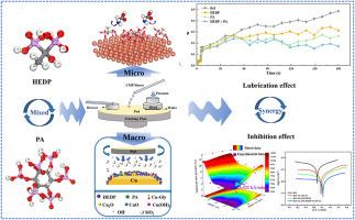
As technology nodes shrink below 10 nm, stricter demands are required for the one-step polishing of copper (Cu) films in ruthenium (Ru)-based Cu interconnects: a high Cu removal rate (RR) and a near-zero Ru RR. In this work, an eco-friendly slurry was newly formulated by combining hydroxyethylethylene diphosphonic acid (HEDP) and phytic acid (PA), both containing phosphate groups, to enhance corrosion inhibition and polishing performance during Cu/Ru CMP. Polishing and electrochemical experiments demonstrated that the synergistic inhibitors achieved a corrosion inhibition efficiency of 96 % for Cu. Under optimized conditions, the material removal rates (MRRs) of Cu and Ru reached 5432 Å/min and 10 Å/min, respectively, with a maximum removal rate selectivity (RRS) of 543:1 and surface roughness (Sqs) of 0.76 nm and 0.53 nm. Contact angle, coefficient of friction (COF), Ultraviolet–visible spectroscopy (UV–Vis), X-ray photoelectron spectroscopy (XPS) analyses confirmed the formation of a protective passivation film on Cu/Ru surfaces from both mechanical and chemical perspectives. Theoretical calculations identified the reactive sites of the inhibitors and simulated their adsorption behavior in a CMP environment, revealing that the synergistic inhibitors exhibited the highest adsorption energy. Without the use of surfactants, the multifunctional synergistic inhibitors improved surface quality through lubrication and passivation effects while reducing reagent consumption. This work provides both theoretical and practical guidance for the design of green and efficient CMP slurries in advanced semiconductor manufacturing.
一种新型的Cu膜CMP浆料在ru基Cu互连中的应用:实验与理论计算的结合
随着技术节点缩小到10纳米以下,对钌基铜互连中铜(Cu)膜的一步抛光提出了更严格的要求:高Cu去除率(RR)和接近于零的Ru RR。在这项工作中,将含有磷酸基团的羟乙基二膦酸(HEDP)和植酸(PA)结合在一起,新配制了一种环保型浆料,以增强Cu/Ru CMP过程中的缓蚀和抛光性能。抛光和电化学实验表明,协同缓蚀剂对Cu的缓蚀效率为96%。在优化条件下,Cu和Ru的材料去除率分别达到5432 Å/min和10 Å/min,最大去除率选择性(RRS)为543:1,表面粗糙度(Sqs)为0.76 nm和0.53 nm。接触角、摩擦系数(COF)、紫外可见光谱(UV-Vis)、x射线光电子能谱(XPS)分析从力学和化学角度证实了Cu/Ru表面形成了保护性钝化膜。理论计算确定了抑制剂的活性位点,并模拟了它们在CMP环境中的吸附行为,结果表明增效抑制剂具有最高的吸附能。在不使用表面活性剂的情况下,多功能协同抑制剂通过润滑和钝化作用改善了表面质量,同时减少了试剂的消耗。本研究为先进半导体制造中绿色高效CMP浆料的设计提供了理论和实践指导。
本文章由计算机程序翻译,如有差异,请以英文原文为准。
求助全文
约1分钟内获得全文
求助全文
来源期刊

Materials Science in Semiconductor Processing
工程技术-材料科学:综合
CiteScore
8.00
自引率
4.90%
发文量
780
审稿时长
42 days
期刊介绍:
Materials Science in Semiconductor Processing provides a unique forum for the discussion of novel processing, applications and theoretical studies of functional materials and devices for (opto)electronics, sensors, detectors, biotechnology and green energy.
Each issue will aim to provide a snapshot of current insights, new achievements, breakthroughs and future trends in such diverse fields as microelectronics, energy conversion and storage, communications, biotechnology, (photo)catalysis, nano- and thin-film technology, hybrid and composite materials, chemical processing, vapor-phase deposition, device fabrication, and modelling, which are the backbone of advanced semiconductor processing and applications.
Coverage will include: advanced lithography for submicron devices; etching and related topics; ion implantation; damage evolution and related issues; plasma and thermal CVD; rapid thermal processing; advanced metallization and interconnect schemes; thin dielectric layers, oxidation; sol-gel processing; chemical bath and (electro)chemical deposition; compound semiconductor processing; new non-oxide materials and their applications; (macro)molecular and hybrid materials; molecular dynamics, ab-initio methods, Monte Carlo, etc.; new materials and processes for discrete and integrated circuits; magnetic materials and spintronics; heterostructures and quantum devices; engineering of the electrical and optical properties of semiconductors; crystal growth mechanisms; reliability, defect density, intrinsic impurities and defects.
 求助内容:
求助内容: 应助结果提醒方式:


