Metal oxide-modified Janus HfSSe monolayers for SF6 decomposition gas detection: A DFT investigation
IF 4.6
3区 工程技术
Q2 ENGINEERING, ELECTRICAL & ELECTRONIC
引用次数: 0
Abstract
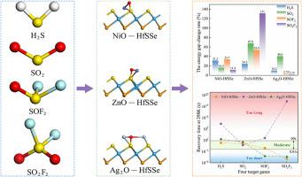
Accurate detection of gases in gas-insulated switchgear (GIS) is essential for maintaining the safe and stable operation of power systems. Density functional theory (DFT) was employed to investigate the adsorption behavior of typical SF6 decomposition gases (H2S, SO2, SOF2, and SO2F2) on NiO-, ZnO-, and Ag2O-modified Janus HfSSe monolayers. All three metal oxides preferentially bind to sulfur sites on the HfSSe surface, forming energetically stable configurations. These modifications significantly enhance the monolayer's conductivity, yielding reduced band gaps of 0.45 eV (NiO), 0.42 eV (ZnO), and 0.37 eV (Ag2O), while simultaneously improving sensitivity and selectivity toward the target gases. At room temperature (298 K), NiO-HfSSe exhibits favorable desorption times for H2S (6.38 s), SO2 (2.95 s), and SOF2 (0.03 s), whereas ZnO- and Ag2O-HfSSe show optimal desorption for SO2 at 0.58 s and 15.67 s, respectively. Combined with short recovery times and significant band gap modulation, NiO-, ZnO-, and Ag2O-modified HfSSe monolayers demonstrate strong potential as reusable, room-temperature gas sensors. This study provides theoretical insight into the application of these modified monolayers for evaluating the insulation status of GIS equipment, laying the groundwork for future experimental validation and optimization of monolayer-based sensors in practical GIS monitoring applications.
用于SF6分解气体检测的金属氧化物修饰Janus HfSSe单层膜:DFT研究
气体绝缘开关设备(GIS)中气体的准确检测对于维持电力系统的安全稳定运行至关重要。采用密度泛函理论(DFT)研究了典型SF6分解气体(H2S、SO2、SOF2和SO2F2)在NiO-、ZnO-和ag20修饰的Janus HfSSe单层膜上的吸附行为。所有三种金属氧化物都优先结合到HfSSe表面的硫位点上,形成能量稳定的构型。这些修饰显著提高了单层膜的电导率,产生了0.45 eV (NiO), 0.42 eV (ZnO)和0.37 eV (Ag2O)的带隙,同时提高了对目标气体的灵敏度和选择性。在室温(298 K)下,NiO-HfSSe对H2S (6.38 s)、SO2 (2.95 s)和SOF2 (0.03 s)具有较好的解吸时间,而ZnO-和ag20 - hfsse对SO2的最佳解吸时间分别为0.58 s和15.67 s。结合较短的恢复时间和显著的带隙调制,NiO-、ZnO-和ag20 -修饰的HfSSe单层显示出作为可重复使用的室温气体传感器的强大潜力。本研究为这些改进的单层传感器在评估GIS设备绝缘状态方面的应用提供了理论见解,为未来在实际GIS监测应用中对单层传感器进行实验验证和优化奠定了基础。
本文章由计算机程序翻译,如有差异,请以英文原文为准。
求助全文
约1分钟内获得全文
求助全文
来源期刊

Materials Science in Semiconductor Processing
工程技术-材料科学:综合
CiteScore
8.00
自引率
4.90%
发文量
780
审稿时长
42 days
期刊介绍:
Materials Science in Semiconductor Processing provides a unique forum for the discussion of novel processing, applications and theoretical studies of functional materials and devices for (opto)electronics, sensors, detectors, biotechnology and green energy.
Each issue will aim to provide a snapshot of current insights, new achievements, breakthroughs and future trends in such diverse fields as microelectronics, energy conversion and storage, communications, biotechnology, (photo)catalysis, nano- and thin-film technology, hybrid and composite materials, chemical processing, vapor-phase deposition, device fabrication, and modelling, which are the backbone of advanced semiconductor processing and applications.
Coverage will include: advanced lithography for submicron devices; etching and related topics; ion implantation; damage evolution and related issues; plasma and thermal CVD; rapid thermal processing; advanced metallization and interconnect schemes; thin dielectric layers, oxidation; sol-gel processing; chemical bath and (electro)chemical deposition; compound semiconductor processing; new non-oxide materials and their applications; (macro)molecular and hybrid materials; molecular dynamics, ab-initio methods, Monte Carlo, etc.; new materials and processes for discrete and integrated circuits; magnetic materials and spintronics; heterostructures and quantum devices; engineering of the electrical and optical properties of semiconductors; crystal growth mechanisms; reliability, defect density, intrinsic impurities and defects.
 求助内容:
求助内容: 应助结果提醒方式:


