Boosted photoelectrochemical water splitting activity by construction of a novel FeVO4/AgVO3 p-n heterostructure
IF 4.6
3区 工程技术
Q2 ENGINEERING, ELECTRICAL & ELECTRONIC
引用次数: 0
Abstract
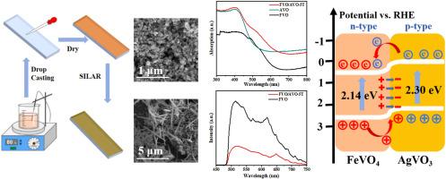
FeVO4 is recognized as a potential photoelectrode material on account of its relatively narrow bandgap and suitable conduction and valence band positions. However, its photoelectrochemical water splitting performance remains unsatisfactory owing to rapid carrier recombination and poor charge transport capabilities. Herein, a novel p-n FeVO4/AgVO3 heterostructure photoanode was developed by depositing p-type AgVO3 nanowires onto n-type FeVO4 nanoporous structures, boosting the PEC properties of the base material. The incorporated AgVO3 nanostructures enhance light absorption in the visible spectrum, facilitate effective electron-hole separation through optimized interfacial charge transport pathways, and simultaneously extend the carrier lifetime. The built-in electric field in the p-n heterostructure promotes more effective separation and directional motion of photoinduced charge carriers. As a result, the transient photocurrent density of the FeVO4/AgVO3 heterojunction photoanode reaches 0.22 mA cm−2, which is 3.35 times that of bare FeVO4 (0.06 mA cm−2). Notably, the incorporation of AgVO3 nanowires significantly improves the photostability of the FeVO4 photoanode. This work provides a feasible strategy from the perspective of interface engineering for designing high-performance FeVO4-based photoelectrodes to enhance photoconversion efficiency.
通过构建新型FeVO4/AgVO3 p-n异质结构提高光电化学水分解活性
由于其相对窄的带隙和合适的导价带位置,FeVO4被认为是一种潜在的光电极材料。然而,由于载流子重组速度快,电荷输运能力差,其光电分解水的性能仍不理想。本文通过在n型FeVO4纳米孔结构上沉积p型AgVO3纳米线,制备了一种新型的p-n型FeVO4/AgVO3异质结构光阳极,提高了基材的PEC性能。加入的AgVO3纳米结构增强了可见光谱的光吸收,通过优化的界面电荷传输途径促进了有效的电子-空穴分离,同时延长了载流子寿命。p-n异质结构中内置的电场促进了光诱导载流子更有效的分离和定向运动。结果表明,FeVO4/AgVO3异质结光阳极的瞬态光电流密度达到0.22 mA cm−2,是裸FeVO4 (0.06 mA cm−2)的3.35倍。值得注意的是,AgVO3纳米线的掺入显著提高了FeVO4光阳极的光稳定性。本工作从界面工程的角度为设计高性能fevo4基光电极提高光转换效率提供了可行的策略。
本文章由计算机程序翻译,如有差异,请以英文原文为准。
求助全文
约1分钟内获得全文
求助全文
来源期刊

Materials Science in Semiconductor Processing
工程技术-材料科学:综合
CiteScore
8.00
自引率
4.90%
发文量
780
审稿时长
42 days
期刊介绍:
Materials Science in Semiconductor Processing provides a unique forum for the discussion of novel processing, applications and theoretical studies of functional materials and devices for (opto)electronics, sensors, detectors, biotechnology and green energy.
Each issue will aim to provide a snapshot of current insights, new achievements, breakthroughs and future trends in such diverse fields as microelectronics, energy conversion and storage, communications, biotechnology, (photo)catalysis, nano- and thin-film technology, hybrid and composite materials, chemical processing, vapor-phase deposition, device fabrication, and modelling, which are the backbone of advanced semiconductor processing and applications.
Coverage will include: advanced lithography for submicron devices; etching and related topics; ion implantation; damage evolution and related issues; plasma and thermal CVD; rapid thermal processing; advanced metallization and interconnect schemes; thin dielectric layers, oxidation; sol-gel processing; chemical bath and (electro)chemical deposition; compound semiconductor processing; new non-oxide materials and their applications; (macro)molecular and hybrid materials; molecular dynamics, ab-initio methods, Monte Carlo, etc.; new materials and processes for discrete and integrated circuits; magnetic materials and spintronics; heterostructures and quantum devices; engineering of the electrical and optical properties of semiconductors; crystal growth mechanisms; reliability, defect density, intrinsic impurities and defects.
 求助内容:
求助内容: 应助结果提醒方式:


