Deep-reactive-ion-etching in X-ray grating fabrication: a review
IF 4.6
3区 工程技术
Q2 ENGINEERING, ELECTRICAL & ELECTRONIC
引用次数: 0
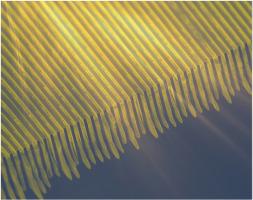
Abstract
The development of grating fabrication shares its journey with the development of X-ray phase contrast imaging. Indeed, the fabrication of gratings with features of sufficiently high aspect ratio is one of the bottlenecks preventing the widespread application of phase contrast imaging in X-ray diagnostics, material science and security. The silicon platform that underlies modern manufacture of integrated circuits, with its well-established technologies for lithography, etching and metal deposition, has the potential to provide high yields and volumes for industrial fabrication of both phase and absorption gratings used in a grating-based X-ray imaging systems. This review article introduces recent developments in the fabrication of high aspect ratio X-ray gratings using ubiquitous clean-room manufacturing tools, focusing on deep reactive ion etching processes. It summarizes the most challenging issues for fabricating features with aspect ratios reaching 70:1, proposing approaches to overcome processing problems and improve product quality.
深反应刻蚀在x射线光栅制造中的研究进展
光栅技术的发展与x射线相衬成像技术的发展是同步的。事实上,具有足够高长宽比的光栅的制造是阻碍相衬成像在x射线诊断、材料科学和安全领域广泛应用的瓶颈之一。作为现代集成电路制造基础的硅平台,凭借其成熟的光刻、蚀刻和金属沉积技术,有潜力为基于光栅的x射线成像系统中使用的相位光栅和吸收光栅的工业制造提供高产量和高产量。本文介绍了利用无所不在的洁净室制造工具制造高纵横比x射线光栅的最新进展,重点介绍了深反应离子刻蚀工艺。总结了制造宽高比达到70:1的特征最具挑战性的问题,提出了克服加工问题和提高产品质量的方法。
本文章由计算机程序翻译,如有差异,请以英文原文为准。
求助全文
约1分钟内获得全文
求助全文
来源期刊

Materials Science in Semiconductor Processing
工程技术-材料科学:综合
CiteScore
8.00
自引率
4.90%
发文量
780
审稿时长
42 days
期刊介绍:
Materials Science in Semiconductor Processing provides a unique forum for the discussion of novel processing, applications and theoretical studies of functional materials and devices for (opto)electronics, sensors, detectors, biotechnology and green energy.
Each issue will aim to provide a snapshot of current insights, new achievements, breakthroughs and future trends in such diverse fields as microelectronics, energy conversion and storage, communications, biotechnology, (photo)catalysis, nano- and thin-film technology, hybrid and composite materials, chemical processing, vapor-phase deposition, device fabrication, and modelling, which are the backbone of advanced semiconductor processing and applications.
Coverage will include: advanced lithography for submicron devices; etching and related topics; ion implantation; damage evolution and related issues; plasma and thermal CVD; rapid thermal processing; advanced metallization and interconnect schemes; thin dielectric layers, oxidation; sol-gel processing; chemical bath and (electro)chemical deposition; compound semiconductor processing; new non-oxide materials and their applications; (macro)molecular and hybrid materials; molecular dynamics, ab-initio methods, Monte Carlo, etc.; new materials and processes for discrete and integrated circuits; magnetic materials and spintronics; heterostructures and quantum devices; engineering of the electrical and optical properties of semiconductors; crystal growth mechanisms; reliability, defect density, intrinsic impurities and defects.
 求助内容:
求助内容: 应助结果提醒方式:


