Chengyao Liang, Wei Hu, Di Peng, Yong Zhou, Yong Wang, Yi Guo, Peng Zhang, Yuhong Wu, Xi Yang and Yong He
{"title":"Defect-passivated InGaZnO/In2O3 stacked thin-film transistors with visible-light-assisted recovery for room-temperature ppb-level NO2 detection†","authors":"Chengyao Liang, Wei Hu, Di Peng, Yong Zhou, Yong Wang, Yi Guo, Peng Zhang, Yuhong Wu, Xi Yang and Yong He","doi":"10.1039/D5TC01843A","DOIUrl":null,"url":null,"abstract":"<p >The hierarchical stacking of oxide semiconductors presents a transformative strategy to address intrinsic defect limitations in amorphous metal oxide semiconductor (MOS)-based thin-film transistors (TFTs). Although conventional MOS-TFTs suffer from high defect densities that degrade carrier mobility and operational stability, the engineered stacking of InGaZnO (IGZO)/In<small><sub>2</sub></small>O<small><sub>3</sub></small> bilayer TFTs demonstrates synergistic electrical and gas sensing enhancements. Fabricated <em>via</em> room-temperature RF magnetron sputtering, the IGZO/In<small><sub>2</sub></small>O<small><sub>3</sub></small> TFTs exhibit superior electrical performance, including a near-zero threshold voltage (≈0 V), enhanced output current density, and reduced hysteresis, which is attributed to the defect passivation mechanism at the interface. These advancements enable low-power, high-stability gas sensors with amplified response signals. Crucially, the IGZO/In<small><sub>2</sub></small>O<small><sub>3</sub></small> TFTs enable dual-mode optical recovery. Visible-light activation replaces UV irradiation, and achieves efficient sensor recovery while maintaining safety and energy efficiency, something unattainable with single-layer In<small><sub>2</sub></small>O<small><sub>3</sub></small> TFTs. The stacked layers further ensure exceptional NO<small><sub>2</sub></small> selectivity towards 50 ppb detection in the temperature range of 25–100 °C and long-term stability, outperforming conventional high-temperature operating MOS gas sensors. Furthermore, this work has the potential to empower forensic science with on-site rapid detection capabilities for trace gaseous evidence, enabling real-time capture and digital evidence archiving of critical targets such as explosive residues and narcotic volatiles through ppb-level sensitivity, visible-light-activated recovery at room temperature, and portability.</p>","PeriodicalId":84,"journal":{"name":"Journal of Materials Chemistry C","volume":" 33","pages":" 17333-17344"},"PeriodicalIF":5.1000,"publicationDate":"2025-07-08","publicationTypes":"Journal Article","fieldsOfStudy":null,"isOpenAccess":false,"openAccessPdf":"","citationCount":"0","resultStr":null,"platform":"Semanticscholar","paperid":null,"PeriodicalName":"Journal of Materials Chemistry C","FirstCategoryId":"1","ListUrlMain":"https://pubs.rsc.org/en/content/articlelanding/2025/tc/d5tc01843a","RegionNum":2,"RegionCategory":"材料科学","ArticlePicture":[],"TitleCN":null,"AbstractTextCN":null,"PMCID":null,"EPubDate":"","PubModel":"","JCR":"Q2","JCRName":"MATERIALS SCIENCE, MULTIDISCIPLINARY","Score":null,"Total":0}
引用次数: 0
Abstract
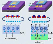
The hierarchical stacking of oxide semiconductors presents a transformative strategy to address intrinsic defect limitations in amorphous metal oxide semiconductor (MOS)-based thin-film transistors (TFTs). Although conventional MOS-TFTs suffer from high defect densities that degrade carrier mobility and operational stability, the engineered stacking of InGaZnO (IGZO)/In2O3 bilayer TFTs demonstrates synergistic electrical and gas sensing enhancements. Fabricated via room-temperature RF magnetron sputtering, the IGZO/In2O3 TFTs exhibit superior electrical performance, including a near-zero threshold voltage (≈0 V), enhanced output current density, and reduced hysteresis, which is attributed to the defect passivation mechanism at the interface. These advancements enable low-power, high-stability gas sensors with amplified response signals. Crucially, the IGZO/In2O3 TFTs enable dual-mode optical recovery. Visible-light activation replaces UV irradiation, and achieves efficient sensor recovery while maintaining safety and energy efficiency, something unattainable with single-layer In2O3 TFTs. The stacked layers further ensure exceptional NO2 selectivity towards 50 ppb detection in the temperature range of 25–100 °C and long-term stability, outperforming conventional high-temperature operating MOS gas sensors. Furthermore, this work has the potential to empower forensic science with on-site rapid detection capabilities for trace gaseous evidence, enabling real-time capture and digital evidence archiving of critical targets such as explosive residues and narcotic volatiles through ppb-level sensitivity, visible-light-activated recovery at room temperature, and portability.
期刊介绍:
The Journal of Materials Chemistry is divided into three distinct sections, A, B, and C, each catering to specific applications of the materials under study:
Journal of Materials Chemistry A focuses primarily on materials intended for applications in energy and sustainability.
Journal of Materials Chemistry B specializes in materials designed for applications in biology and medicine.
Journal of Materials Chemistry C is dedicated to materials suitable for applications in optical, magnetic, and electronic devices.
Example topic areas within the scope of Journal of Materials Chemistry C are listed below. This list is neither exhaustive nor exclusive.
Bioelectronics
Conductors
Detectors
Dielectrics
Displays
Ferroelectrics
Lasers
LEDs
Lighting
Liquid crystals
Memory
Metamaterials
Multiferroics
Photonics
Photovoltaics
Semiconductors
Sensors
Single molecule conductors
Spintronics
Superconductors
Thermoelectrics
Topological insulators
Transistors

 求助内容:
求助内容: 应助结果提醒方式:


