Effect of native oxidation and hydroxidation on earth-abundant ZnSnN2 grown by reactive RF magnetron sputtering
IF 4.6
3区 工程技术
Q2 ENGINEERING, ELECTRICAL & ELECTRONIC
引用次数: 0
Abstract
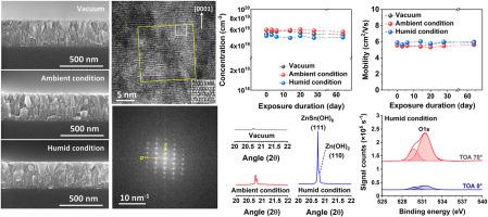
II-IV-N2 semiconductors such as ZnSnN2 have emerged as promising earth-abundant materials, but their heterovalent bonding structure is more susceptible to oxidation and hydroxidation than conventional III-nitrides. In this study, we focus on native oxidation and hydroxidation of ZnSnN2 thin films grown by RF magnetron sputtering and investigate the roles of atmospheric moisture and oxygen in material degradation. By exposing ZnSnN2 to controlled environments with varying humidity, we observed significant oxidation and hydroxidation under humid conditions, as confirmed by energy-dispersive X-ray spectroscopy (EDS), X-ray diffraction (XRD), and X-ray photoelectron spectroscopy (XPS) analysis. In particular, the formation of the oxides (SnO2) and hydroxides (Zn(OH)2 and ZnSn(OH)6) on the surface remained unaffected, indicating surface-limited oxidation. Angle-resolved XPS revealed a self-passivating oxide and hydroxide layer that prevents deep oxidation and hydroxidation. These findings demonstrate a self-limiting property of an oxide and hydroxide layer formed under humid conditions, providing valuable insight into the environmental stability of ZnSnN2.
天然氧化和氢化作用对反应性射频磁控溅射制备地球富集ZnSnN2的影响
像ZnSnN2这样的II-IV-N2半导体已经成为一种很有前途的地球丰富材料,但它们的异价键结构比传统的iii -氮化物更容易被氧化和羟基化。在这项研究中,我们重点研究了射频磁控溅射生长的ZnSnN2薄膜的天然氧化和羟基化,并研究了大气湿度和氧气在材料降解中的作用。通过将ZnSnN2暴露在不同湿度的受控环境中,我们观察到在潮湿条件下存在明显的氧化和氢化反应,并通过能量色散x射线能谱(EDS)、x射线衍射(XRD)和x射线光电子能谱(XPS)分析证实了这一点。特别是,表面氧化物(SnO2)和氢氧化物(Zn(OH)2和ZnSn(OH)6)的形成没有受到影响,表明表面有限氧化。角度分辨XPS发现了一种自钝化的氧化物和氢氧化物层,可以防止深度氧化和羟基化。这些发现证明了在潮湿条件下形成的氧化物和氢氧化物层的自限制特性,为ZnSnN2的环境稳定性提供了有价值的见解。
本文章由计算机程序翻译,如有差异,请以英文原文为准。
求助全文
约1分钟内获得全文
求助全文
来源期刊

Materials Science in Semiconductor Processing
工程技术-材料科学:综合
CiteScore
8.00
自引率
4.90%
发文量
780
审稿时长
42 days
期刊介绍:
Materials Science in Semiconductor Processing provides a unique forum for the discussion of novel processing, applications and theoretical studies of functional materials and devices for (opto)electronics, sensors, detectors, biotechnology and green energy.
Each issue will aim to provide a snapshot of current insights, new achievements, breakthroughs and future trends in such diverse fields as microelectronics, energy conversion and storage, communications, biotechnology, (photo)catalysis, nano- and thin-film technology, hybrid and composite materials, chemical processing, vapor-phase deposition, device fabrication, and modelling, which are the backbone of advanced semiconductor processing and applications.
Coverage will include: advanced lithography for submicron devices; etching and related topics; ion implantation; damage evolution and related issues; plasma and thermal CVD; rapid thermal processing; advanced metallization and interconnect schemes; thin dielectric layers, oxidation; sol-gel processing; chemical bath and (electro)chemical deposition; compound semiconductor processing; new non-oxide materials and their applications; (macro)molecular and hybrid materials; molecular dynamics, ab-initio methods, Monte Carlo, etc.; new materials and processes for discrete and integrated circuits; magnetic materials and spintronics; heterostructures and quantum devices; engineering of the electrical and optical properties of semiconductors; crystal growth mechanisms; reliability, defect density, intrinsic impurities and defects.
 求助内容:
求助内容: 应助结果提醒方式:


