Enhanced oxygen sensing using the Pb-doped SnS nanostructures: Overcoming the humidity challenges
IF 4.6
3区 工程技术
Q2 ENGINEERING, ELECTRICAL & ELECTRONIC
引用次数: 0
Abstract
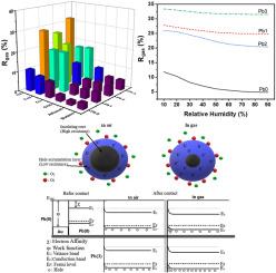
In this research, the gas and humidity sensing properties of Pb-doped SnS nanostructures synthesized via a sonochemical method were investigated. The study aims to enhance oxygen sensing performance and overcome challenges posed by humidity interference. Various concentrations of Pb were incorporated into the SnS nanostructures, and their structural, morphological, and optical properties were thoroughly analyzed. Our results indicate that Pb doping influences the crystallite size and strain, enhancing gas adsorption properties and improving sensor response. The Pb-doped sensors demonstrated better oxygen sensing performance, with the Pb3 sample showing the highest response at 170 °C. The Pb-doped sensors exhibited a lower humidity response compared to the undoped sensor. For example, the Pb3 sample exhibited responses of 32 % and 9.5 % to oxygen and humidity, respectively, while the Pb0 sample showed responses of 11 % and 190 % to oxygen and humidity, respectively. The sensors show good stability and reproducibility, making them suitable for real-world applications where both gas and humidity must be detected simultaneously. These findings open new avenues for developing efficient, low-cost sensors for environmental monitoring and industrial use.
利用掺杂铅的SnS纳米结构增强氧传感:克服湿度挑战
在本研究中,研究了通过声化学方法合成的掺杂铅的SnS纳米结构的气体和湿度传感性能。该研究旨在提高氧传感性能,克服湿度干扰带来的挑战。将不同浓度的Pb加入到SnS纳米结构中,并对其结构、形态和光学性质进行了全面分析。结果表明,Pb掺杂影响了晶体尺寸和应变,增强了气体吸附性能,改善了传感器响应。铅掺杂的传感器表现出更好的氧传感性能,其中Pb3样品在170°C时表现出最高的响应。与未掺杂的传感器相比,掺杂铅的传感器表现出较低的湿度响应。例如,Pb3样品对氧气和湿度的响应分别为32%和9.5%,而Pb0样品对氧气和湿度的响应分别为11%和190%。该传感器具有良好的稳定性和可重复性,适用于必须同时检测气体和湿度的实际应用。这些发现为开发用于环境监测和工业用途的高效、低成本传感器开辟了新的途径。
本文章由计算机程序翻译,如有差异,请以英文原文为准。
求助全文
约1分钟内获得全文
求助全文
来源期刊

Materials Science in Semiconductor Processing
工程技术-材料科学:综合
CiteScore
8.00
自引率
4.90%
发文量
780
审稿时长
42 days
期刊介绍:
Materials Science in Semiconductor Processing provides a unique forum for the discussion of novel processing, applications and theoretical studies of functional materials and devices for (opto)electronics, sensors, detectors, biotechnology and green energy.
Each issue will aim to provide a snapshot of current insights, new achievements, breakthroughs and future trends in such diverse fields as microelectronics, energy conversion and storage, communications, biotechnology, (photo)catalysis, nano- and thin-film technology, hybrid and composite materials, chemical processing, vapor-phase deposition, device fabrication, and modelling, which are the backbone of advanced semiconductor processing and applications.
Coverage will include: advanced lithography for submicron devices; etching and related topics; ion implantation; damage evolution and related issues; plasma and thermal CVD; rapid thermal processing; advanced metallization and interconnect schemes; thin dielectric layers, oxidation; sol-gel processing; chemical bath and (electro)chemical deposition; compound semiconductor processing; new non-oxide materials and their applications; (macro)molecular and hybrid materials; molecular dynamics, ab-initio methods, Monte Carlo, etc.; new materials and processes for discrete and integrated circuits; magnetic materials and spintronics; heterostructures and quantum devices; engineering of the electrical and optical properties of semiconductors; crystal growth mechanisms; reliability, defect density, intrinsic impurities and defects.
 求助内容:
求助内容: 应助结果提醒方式:


