Stability of masking materials for pattern transfer of lithographic masks into fused silica by atmospheric pressure plasma jet etching
IF 3.1
Q2 ENGINEERING, ELECTRICAL & ELECTRONIC
引用次数: 0
Abstract
Masking of thin films and bulk materials is traditionally applied for the transfer of micron patterns into the functional material according to the requirements of the application. For optical purposes, lithographically produced micron patterns are transferred by plasma/ion etching, which is a traditional technology in microelectronics and other micron technologies. However, pattern transfer by atmospheric pressure plasma etching can help to save time and cost for a future sustainable production. Therefore, the pattern transfer of lithographic resist masks into fused silica using atmospheric pressure reactive plasma jets (APPJ) was studied as a new approach of micropatterning.
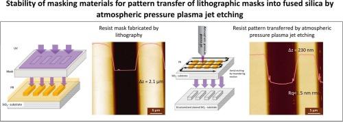
First the etch rates of the potential masking materials, e.g. photoresists, as well as of fused silica as substrate are studied in dependence on the APPJ etching parameters, in particular on the gas composition (O2/CF4) and the dwell time of the APPJ tool's footprint. Typical etch rates of the masking materials are in the range of 140 to 370 nm·s−1 whereas the fused silica has a rate of 25 to 80 nm·s−1. The surface morphology of masking materials changes during etching and features additional nanoscale roughness and waviness. The surface roughness of the etched masking materials and the fused silica are 2 to 5 nm rms and 1.5 nm rms for etch depths of ∼3000 nm and ∼ 600 nm, respectively. Finally, the pattern transfer by APPJ of a diffraction grating with a period of 15 μm, depth of 230 nm and a roughness below 2 nm rms into fused silica was demonstrated.
常压等离子体喷射蚀刻用于熔融二氧化硅光刻模板图案转移的掩蔽材料的稳定性
薄膜和块状材料的掩蔽传统上用于根据应用的要求将微米图案转移到功能材料中。为了光学目的,光刻产生的微米图案通过等离子体/离子蚀刻转移,这是微电子和其他微米技术中的传统技术。然而,通过大气压等离子蚀刻的图案转移可以帮助节省时间和成本,为未来的可持续生产。因此,利用常压反应等离子体射流(APPJ)将光刻抗蚀剂掩模的图案转移到熔融二氧化硅中作为一种微图案的新方法进行了研究。首先,研究了潜在掩蔽材料(如光刻胶)以及作为衬底的熔融二氧化硅的蚀刻速率与APPJ蚀刻参数的关系,特别是与气体组成(O2/CF4)和APPJ工具足迹的停留时间的关系。掩蔽材料的典型蚀刻速率在140 ~ 370 nm·s−1范围内,而熔融石英的蚀刻速率为25 ~ 80 nm·s−1。在蚀刻过程中,掩蔽材料的表面形貌发生了变化,并具有额外的纳米级粗糙度和波浪形。当刻蚀深度为~ 3000 nm和~ 600 nm时,刻蚀掩蔽材料和熔融二氧化硅的表面粗糙度分别为2 ~ 5 nm rms和1.5 nm rms。最后,利用APPJ证明了周期为15 μm、深度为230 nm、粗糙度小于2 nm rms的衍射光栅在熔融石英中的图案转移。
本文章由计算机程序翻译,如有差异,请以英文原文为准。
求助全文
约1分钟内获得全文
求助全文
来源期刊
Micro and Nano Engineering
Engineering-Electrical and Electronic Engineering
CiteScore
3.30
自引率
0.00%
发文量
67
审稿时长
80 days
 求助内容:
求助内容: 应助结果提醒方式:


