Zhanibek Bizak, Harold F. Mazo-Mantilla, Linqu Luo, Camelia Florica, Georgian Melinte, Thomas D. Anthopoulos, Khaled N. Salama
{"title":"Arithmetic Logic Unit Circuit Based on Zinc Oxide Nanogap Schottky Diodes","authors":"Zhanibek Bizak, Harold F. Mazo-Mantilla, Linqu Luo, Camelia Florica, Georgian Melinte, Thomas D. Anthopoulos, Khaled N. Salama","doi":"10.1002/aelm.202400940","DOIUrl":null,"url":null,"abstract":"<p>The intrinsic high non-linearity of Schottky diodes with the latest improvements in performance, material, and design novelties have made them invaluable in the emerging devices ecosystem. However, the reported studies on diodes based on 2D and metal-oxide semiconductors for digital circuits are limited to basic logic gates. The Schottky diodes-based integrated circuit feasibility and scalability discussions are lacking. In this work, the large throughput and cost-effective adhesion lithography in tandem with the solution-based method is used to fabricate integrated functional circuits for Arithmetic Logic Unit (ALU). The self-aligned nanogap separation between interdigitated coplanar aluminum (Al) and gold (Au) electrodes is uniform throughout the fabricated diode width, resulting in a high rectification ratio of 5 × 10<sup>6</sup>. The fundamental logic AND, OR, and XOR gates based on nanogap Schottky diodes are fabricated, from which arbitrary logic and arithmetic functional circuits can be constructed. To demonstrate the large-area integration, a 3-bit Binary Shifter circuit is implemented. The measurement-based Keysight ADS diode model is used to design a complete 4-bit ALU circuit. The excellent circuit-level performance, large-area scalability, design flexibility, and cost-efficiency of logic circuits based on nanogap Schottky diodes make them promising candidates for future Internet of Things applications.</p>","PeriodicalId":110,"journal":{"name":"Advanced Electronic Materials","volume":"11 12","pages":""},"PeriodicalIF":5.3000,"publicationDate":"2025-07-13","publicationTypes":"Journal Article","fieldsOfStudy":null,"isOpenAccess":false,"openAccessPdf":"https://onlinelibrary.wiley.com/doi/epdf/10.1002/aelm.202400940","citationCount":"0","resultStr":null,"platform":"Semanticscholar","paperid":null,"PeriodicalName":"Advanced Electronic Materials","FirstCategoryId":"88","ListUrlMain":"https://advanced.onlinelibrary.wiley.com/doi/10.1002/aelm.202400940","RegionNum":2,"RegionCategory":"材料科学","ArticlePicture":[],"TitleCN":null,"AbstractTextCN":null,"PMCID":null,"EPubDate":"","PubModel":"","JCR":"Q2","JCRName":"MATERIALS SCIENCE, MULTIDISCIPLINARY","Score":null,"Total":0}
引用次数: 0
Abstract
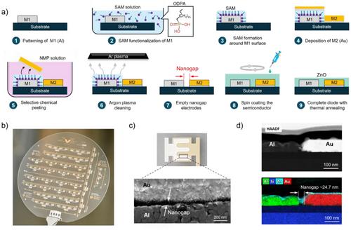
The intrinsic high non-linearity of Schottky diodes with the latest improvements in performance, material, and design novelties have made them invaluable in the emerging devices ecosystem. However, the reported studies on diodes based on 2D and metal-oxide semiconductors for digital circuits are limited to basic logic gates. The Schottky diodes-based integrated circuit feasibility and scalability discussions are lacking. In this work, the large throughput and cost-effective adhesion lithography in tandem with the solution-based method is used to fabricate integrated functional circuits for Arithmetic Logic Unit (ALU). The self-aligned nanogap separation between interdigitated coplanar aluminum (Al) and gold (Au) electrodes is uniform throughout the fabricated diode width, resulting in a high rectification ratio of 5 × 10⁶. The fundamental logic AND, OR, and XOR gates based on nanogap Schottky diodes are fabricated, from which arbitrary logic and arithmetic functional circuits can be constructed. To demonstrate the large-area integration, a 3-bit Binary Shifter circuit is implemented. The measurement-based Keysight ADS diode model is used to design a complete 4-bit ALU circuit. The excellent circuit-level performance, large-area scalability, design flexibility, and cost-efficiency of logic circuits based on nanogap Schottky diodes make them promising candidates for future Internet of Things applications.
期刊介绍:
Advanced Electronic Materials is an interdisciplinary forum for peer-reviewed, high-quality, high-impact research in the fields of materials science, physics, and engineering of electronic and magnetic materials. It includes research on physics and physical properties of electronic and magnetic materials, spintronics, electronics, device physics and engineering, micro- and nano-electromechanical systems, and organic electronics, in addition to fundamental research.


 求助内容:
求助内容: 应助结果提醒方式:


