Muhammad Abubakr, Muhammad Hamza Pervez, Arslan Rehmat, Muhammad Asghar Khan, Ehsan Elahi, Muhammad Asim, Muhammad Rabeel, Muhammad Nasim, Zeesham Abbas, Malik Abdul Rehman, Aize Hao, Jonghwa Eom, Shania Rehman and Muhammad Farooq Khan
{"title":"UV to NIR photodetection in lateral homojunction PN diode of WSe2 achieved via IGZO sputtering†","authors":"Muhammad Abubakr, Muhammad Hamza Pervez, Arslan Rehmat, Muhammad Asghar Khan, Ehsan Elahi, Muhammad Asim, Muhammad Rabeel, Muhammad Nasim, Zeesham Abbas, Malik Abdul Rehman, Aize Hao, Jonghwa Eom, Shania Rehman and Muhammad Farooq Khan","doi":"10.1039/D4TC04705B","DOIUrl":null,"url":null,"abstract":"<p >Nano-devices based on two-dimensional (2D) semiconductor materials encourage the development of high-performance homogeneous junctions owing to their remarkable electronic and optoelectronic properties. Herein, we fabricated an atomically thin WSe<small><sub>2</sub></small> (∼4.8 nm) lateral homojunction PN diode through the deposition of indium gallium zinc oxide (IGZO) <em>via</em> sputtering. Pristine WSe<small><sub>2</sub></small> exhibited dominant p-type semiconductor behavior, while IGZO-deposited WSe<small><sub>2</sub></small> demonstrated n-type behavior, revealing that IGZO altered the carrier polarity of WSe<small><sub>2</sub></small> from p- to n-type. Furthermore, we investigated gate-dependent <em>I</em>–<em>V</em> curves of the lateral homojunction PN (p-WSe<small><sub>2</sub></small>/n-IGZO·WSe<small><sub>2</sub></small>) diode in the dark based on a single WSe<small><sub>2</sub></small> flake, which showed a promising current rectification ratio (∼1.6 × 10<small><sup>4</sup></small>) and ideality factor (∼1.23) at <em>V</em><small><sub>BG</sub></small> = −30 V, respectively. Subsequently, to explore the photodiode characteristics, we irradiated the lateral homojunction PN diode of WSe<small><sub>2</sub></small> under ultra-violet (UV) to near-infrared (NIR) light (365, 530, and 850 nm). The <em>I</em>–<em>V</em> curves of the diode significantly changed under light irradiation, and the open circuit voltage (<em>V</em><small><sub>oc</sub></small> = 202, 166, and 134 mV) and short circuit current (<em>I</em><small><sub>sc</sub></small> = 320, 171, and 122 nA) values increased under illumination of a laser of small wavelength (365, 530, and 850 nm). Furthermore, we investigated the time-dependent photoresponse behavior of the diode under different laser lights. This demonstrated promising photoresponsivity (<em>R</em><small><sub>Ph</sub></small> = 40.1 A W<small><sup>−1</sup></small>) and external quantum efficiency (EQE = 13 634%) at <em>λ</em> = 365 nm and <em>V</em><small><sub>BG</sub></small> = 15 V. Hence, our lateral homojunction PN diode WSe<small><sub>2</sub></small>–IGZO/WSe<small><sub>2</sub></small> shows great potential for next-generation electronic devices at the nanoscale level.</p>","PeriodicalId":84,"journal":{"name":"Journal of Materials Chemistry C","volume":" 17","pages":" 8544-8552"},"PeriodicalIF":5.1000,"publicationDate":"2025-03-11","publicationTypes":"Journal Article","fieldsOfStudy":null,"isOpenAccess":false,"openAccessPdf":"https://pubs.rsc.org/en/content/articlepdf/2025/tc/d4tc04705b?page=search","citationCount":"0","resultStr":null,"platform":"Semanticscholar","paperid":null,"PeriodicalName":"Journal of Materials Chemistry C","FirstCategoryId":"1","ListUrlMain":"https://pubs.rsc.org/en/content/articlelanding/2025/tc/d4tc04705b","RegionNum":2,"RegionCategory":"材料科学","ArticlePicture":[],"TitleCN":null,"AbstractTextCN":null,"PMCID":null,"EPubDate":"","PubModel":"","JCR":"Q2","JCRName":"MATERIALS SCIENCE, MULTIDISCIPLINARY","Score":null,"Total":0}
引用次数: 0
Abstract
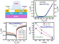
Nano-devices based on two-dimensional (2D) semiconductor materials encourage the development of high-performance homogeneous junctions owing to their remarkable electronic and optoelectronic properties. Herein, we fabricated an atomically thin WSe2 (∼4.8 nm) lateral homojunction PN diode through the deposition of indium gallium zinc oxide (IGZO) via sputtering. Pristine WSe2 exhibited dominant p-type semiconductor behavior, while IGZO-deposited WSe2 demonstrated n-type behavior, revealing that IGZO altered the carrier polarity of WSe2 from p- to n-type. Furthermore, we investigated gate-dependent I–V curves of the lateral homojunction PN (p-WSe2/n-IGZO·WSe2) diode in the dark based on a single WSe2 flake, which showed a promising current rectification ratio (∼1.6 × 10⁴) and ideality factor (∼1.23) at VBG = −30 V, respectively. Subsequently, to explore the photodiode characteristics, we irradiated the lateral homojunction PN diode of WSe2 under ultra-violet (UV) to near-infrared (NIR) light (365, 530, and 850 nm). The I–V curves of the diode significantly changed under light irradiation, and the open circuit voltage (Voc = 202, 166, and 134 mV) and short circuit current (Isc = 320, 171, and 122 nA) values increased under illumination of a laser of small wavelength (365, 530, and 850 nm). Furthermore, we investigated the time-dependent photoresponse behavior of the diode under different laser lights. This demonstrated promising photoresponsivity (RPh = 40.1 A W−1) and external quantum efficiency (EQE = 13 634%) at λ = 365 nm and VBG = 15 V. Hence, our lateral homojunction PN diode WSe2–IGZO/WSe2 shows great potential for next-generation electronic devices at the nanoscale level.
期刊介绍:
The Journal of Materials Chemistry is divided into three distinct sections, A, B, and C, each catering to specific applications of the materials under study:
Journal of Materials Chemistry A focuses primarily on materials intended for applications in energy and sustainability.
Journal of Materials Chemistry B specializes in materials designed for applications in biology and medicine.
Journal of Materials Chemistry C is dedicated to materials suitable for applications in optical, magnetic, and electronic devices.
Example topic areas within the scope of Journal of Materials Chemistry C are listed below. This list is neither exhaustive nor exclusive.
Bioelectronics
Conductors
Detectors
Dielectrics
Displays
Ferroelectrics
Lasers
LEDs
Lighting
Liquid crystals
Memory
Metamaterials
Multiferroics
Photonics
Photovoltaics
Semiconductors
Sensors
Single molecule conductors
Spintronics
Superconductors
Thermoelectrics
Topological insulators
Transistors

 求助内容:
求助内容: 应助结果提醒方式:


