Ohmic Response in BiFeO3 Domain Walls by Submicron‐Scale Four‐Point Probe Resistance Measurements
IF 5.3
2区 材料科学
Q2 MATERIALS SCIENCE, MULTIDISCIPLINARY
引用次数: 0
Abstract
Conducting domain walls (DWs) hold promise for novel electronic devices. However, the electrical characterization of DWs is challenging because of their nanoscale dimensions and the large driving fields that are typically required due to the high resistance of the hosting material. Until now, lateral transport measurements of DWs have mainly been realized using lateral nano‐gap electrode structures or conventional conducting atomic force microscopy (cAFM). Here, a non‐destructive and lithography‐free method is reported for lateral transport measurement of DWs, which is applied to BiFeO
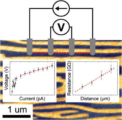
导电畴壁(DWs)有望用于新型电子设备。然而,DWs 的电学表征具有挑战性,因为它们具有纳米级尺寸,而且由于寄主材料的高电阻,通常需要较大的驱动场。迄今为止,DWs 的横向传输测量主要通过横向纳米间隙电极结构或传统的导电原子力显微镜(cAFM)来实现。本文报告了一种非破坏性和免光刻的 DW 横向传输测量方法,该方法利用亚微米级多点探针 (MPP) 应用于 BiFeO3 (BFO) 薄膜。使用不同的独立偏压探针针尖,可以在不同的横向距离上进行两点和四点测量,最小针尖间距为几百纳米。这些测量结果揭示了 BFO 薄膜中 71° DW 的铁弹性/铁电性欧姆行为,以及单个 DW(不含引线电阻和接触电阻)的首个共线四点电阻率值。这些发现有助于更好地理解 DW 的传导,突出了 MPPs 在横向传输测量包含导电甚至记忆性纳米级网络的材料方面的能力。
本文章由计算机程序翻译,如有差异,请以英文原文为准。
求助全文
约1分钟内获得全文
求助全文
来源期刊

Advanced Electronic Materials
NANOSCIENCE & NANOTECHNOLOGYMATERIALS SCIE-MATERIALS SCIENCE, MULTIDISCIPLINARY
CiteScore
11.00
自引率
3.20%
发文量
433
期刊介绍:
Advanced Electronic Materials is an interdisciplinary forum for peer-reviewed, high-quality, high-impact research in the fields of materials science, physics, and engineering of electronic and magnetic materials. It includes research on physics and physical properties of electronic and magnetic materials, spintronics, electronics, device physics and engineering, micro- and nano-electromechanical systems, and organic electronics, in addition to fundamental research.
 求助内容:
求助内容: 应助结果提醒方式:


