Preetam Dacha, Vaidehi Lapalikar, Anju Kumari Rohitlal, Mike Hambsch, Michael Ruck, Stefan C. B. Mannsfeld
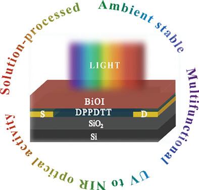
{"title":"Solution-Processed Bismuth Oxide Iodide/Organic-Semiconductor Heterojunction for UV–vis-NIR Photoresponsive Electronics","authors":"Preetam Dacha, Vaidehi Lapalikar, Anju Kumari Rohitlal, Mike Hambsch, Michael Ruck, Stefan C. B. Mannsfeld","doi":"10.1002/aelm.202400726","DOIUrl":null,"url":null,"abstract":"<p>The emerging light absorber material bismuth oxide iodide BiOI, possesses convenient solution processibility and excellent chemical stability under ambient conditions along with a high light absorption coefficient reaching 5·10<sup>4</sup> cm<sup>−1</sup>. Classified as “defect-tolerant,” BiOI is considered a green and low-cost alternative to lead-halide perovskites in optoelectronic devices. Its investigation in photoresponsive electronic devices, however, is limited due to its anisotropic carrier mobility and unique morphology in thin films. To utilize the advantageous properties of BiOI, in this work, it is integrated into a phototransistor as a bilayer heterojunction with the organic semiconductor DPPDTT. The smooth interfaces and higher carrier mobility of DPPDTT compared to BiOI and its hydrophobic nature enable their synergistic hybridization in a heterojunction that is optically active from the UV to the NIR region. The unencapsulated heterojunction phototransistors are stable for at least three months under atmospheric conditions. They show a high <i>I</i><sub>light</sub>/<i>I</i><sub>dark</sub> current ratio of over 10<sup>4</sup> at only 0.7 mW·cm<sup>−2</sup> irradiation intensity at all investigated wavelengths, and a specific detectivity up to 5·10<sup>12</sup> Jones. Initial synaptic measurements additionally reveal a neuromorphic behavior in the devices. This work charts a course towards the realization of cost-effective high-performance photoresponsive electronics for diverse applications.</p>","PeriodicalId":110,"journal":{"name":"Advanced Electronic Materials","volume":"11 7","pages":""},"PeriodicalIF":5.3000,"publicationDate":"2025-02-19","publicationTypes":"Journal Article","fieldsOfStudy":null,"isOpenAccess":false,"openAccessPdf":"https://onlinelibrary.wiley.com/doi/epdf/10.1002/aelm.202400726","citationCount":"0","resultStr":null,"platform":"Semanticscholar","paperid":null,"PeriodicalName":"Advanced Electronic Materials","FirstCategoryId":"88","ListUrlMain":"https://onlinelibrary.wiley.com/doi/10.1002/aelm.202400726","RegionNum":2,"RegionCategory":"材料科学","ArticlePicture":[],"TitleCN":null,"AbstractTextCN":null,"PMCID":null,"EPubDate":"","PubModel":"","JCR":"Q2","JCRName":"MATERIALS SCIENCE, MULTIDISCIPLINARY","Score":null,"Total":0}
引用次数: 0
Abstract
The emerging light absorber material bismuth oxide iodide BiOI, possesses convenient solution processibility and excellent chemical stability under ambient conditions along with a high light absorption coefficient reaching 5·104 cm−1. Classified as “defect-tolerant,” BiOI is considered a green and low-cost alternative to lead-halide perovskites in optoelectronic devices. Its investigation in photoresponsive electronic devices, however, is limited due to its anisotropic carrier mobility and unique morphology in thin films. To utilize the advantageous properties of BiOI, in this work, it is integrated into a phototransistor as a bilayer heterojunction with the organic semiconductor DPPDTT. The smooth interfaces and higher carrier mobility of DPPDTT compared to BiOI and its hydrophobic nature enable their synergistic hybridization in a heterojunction that is optically active from the UV to the NIR region. The unencapsulated heterojunction phototransistors are stable for at least three months under atmospheric conditions. They show a high Ilight/Idark current ratio of over 104 at only 0.7 mW·cm−2 irradiation intensity at all investigated wavelengths, and a specific detectivity up to 5·1012 Jones. Initial synaptic measurements additionally reveal a neuromorphic behavior in the devices. This work charts a course towards the realization of cost-effective high-performance photoresponsive electronics for diverse applications.
期刊介绍:
Advanced Electronic Materials is an interdisciplinary forum for peer-reviewed, high-quality, high-impact research in the fields of materials science, physics, and engineering of electronic and magnetic materials. It includes research on physics and physical properties of electronic and magnetic materials, spintronics, electronics, device physics and engineering, micro- and nano-electromechanical systems, and organic electronics, in addition to fundamental research.


 求助内容:
求助内容: 应助结果提醒方式:


