High‐Frequency Inductors by Co‐Design Optimization of Self‐Rolled‐up Membrane Technology
IF 5.3
2区 材料科学
Q2 MATERIALS SCIENCE, MULTIDISCIPLINARY
引用次数: 0
Abstract
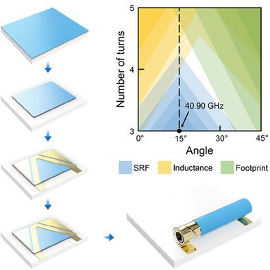
Self‐rolled‐up membrane (S‐RuM) 3D microtube inductors represent a significant advancement in miniaturization for radio frequency (RF) integrated circuit applications, particularly internet‐of‐things and 5G/6G communications. These inductors have excellent high‐frequency performance due to better confinement of the magnetic field and weak dependence on substrate conductivity. However, previously reported S‐RuM inductor frequencies are limited by the crosstalk capacitance between overlapping metal strips between rolled‐up turns. This work advances S‐RuM inductor design by co‐optimizing inductance, frequency, and footprint, leading to significant reductions in crosstalk capacitance and enhancements in maximum operating frequencies. Design intricacies tailored to the unique structure of S‐RuM inductors are thoroughly addressed, particularly by mapping the angle of the rolled‐up inductor strips with respect to the number of turns. Self‐resonance frequencies as high as 40–53 GHz (instrument testing limit) are reported for 2–5 rolled‐up turns, demonstrating increases of over 15 GHz from previous S‐RuM inductors. These designs, with footprints of 0.02–0.56 mm
求助全文
约1分钟内获得全文
求助全文
来源期刊

Advanced Electronic Materials
NANOSCIENCE & NANOTECHNOLOGYMATERIALS SCIE-MATERIALS SCIENCE, MULTIDISCIPLINARY
CiteScore
11.00
自引率
3.20%
发文量
433
期刊介绍:
Advanced Electronic Materials is an interdisciplinary forum for peer-reviewed, high-quality, high-impact research in the fields of materials science, physics, and engineering of electronic and magnetic materials. It includes research on physics and physical properties of electronic and magnetic materials, spintronics, electronics, device physics and engineering, micro- and nano-electromechanical systems, and organic electronics, in addition to fundamental research.
 求助内容:
求助内容: 应助结果提醒方式:


