Development of a Nb-Based Semiconductor-Superconductor Hybrid 2DEG Platform

IF 5.3 2区 材料科学 Q2 MATERIALS SCIENCE, MULTIDISCIPLINARY
Sjoerd Telkamp, Tommaso Antonelli, Clemens Todt, Manuel Hinderling, Marco Coraiola, Daniel Haxell, Sofieke C. ten Kate, Deividas Sabonis, Peng Zeng, Rüdiger Schott, Erik Cheah, Christian Reichl, Fabrizio Nichele, Filip Krizek, Werner Wegscheider
{"title":"Development of a Nb-Based Semiconductor-Superconductor Hybrid 2DEG Platform","authors":"Sjoerd Telkamp, Tommaso Antonelli, Clemens Todt, Manuel Hinderling, Marco Coraiola, Daniel Haxell, Sofieke C. ten Kate, Deividas Sabonis, Peng Zeng, Rüdiger Schott, Erik Cheah, Christian Reichl, Fabrizio Nichele, Filip Krizek, Werner Wegscheider","doi":"10.1002/aelm.202400687","DOIUrl":null,"url":null,"abstract":"Semiconductor-superconductor hybrid materials are used as a platform to realize Andreev bound states, which hold great promise for quantum applications. These states require transparent interfaces between the semiconductor and superconductor, which are typically realized by in-situ deposition of an Al superconducting layer. Here a hybrid material is presented, based on an InAs 2D electron gas (2DEG) combined with in-situ deposited Nb and NbTi superconductors, which offer a larger operating range in temperature and magnetic field due to their larger superconducting gap. The inherent difficulty associated with the formation of an amorphous interface between III-V semiconductors and Nb-based superconductors is addressed by introducing a 7 nm Al interlayer. The Al interlayer provides an epitaxial connection between an in-situ magnetron sputtered Nb or NbTi thin film and a shallow InAs 2DEG. This metal-to-metal epitaxy is achieved by optimization of the material stack and results in an induced superconducting gap of approximately 1 meV, determined from transport measurements of superconductor-semiconductor Josephson junctions. This induced gap is approximately five times larger than the values reported for Al-based hybrid materials and indicates the formation of highly-transparent interfaces that are required in high-quality hybrid material platforms.","PeriodicalId":110,"journal":{"name":"Advanced Electronic Materials","volume":"2 1","pages":""},"PeriodicalIF":5.3000,"publicationDate":"2025-01-15","publicationTypes":"Journal Article","fieldsOfStudy":null,"isOpenAccess":false,"openAccessPdf":"","citationCount":"0","resultStr":null,"platform":"Semanticscholar","paperid":null,"PeriodicalName":"Advanced Electronic Materials","FirstCategoryId":"88","ListUrlMain":"https://doi.org/10.1002/aelm.202400687","RegionNum":2,"RegionCategory":"材料科学","ArticlePicture":[],"TitleCN":null,"AbstractTextCN":null,"PMCID":null,"EPubDate":"","PubModel":"","JCR":"Q2","JCRName":"MATERIALS SCIENCE, MULTIDISCIPLINARY","Score":null,"Total":0}
引用次数: 0

Abstract

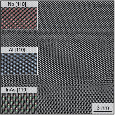
Semiconductor-superconductor hybrid materials are used as a platform to realize Andreev bound states, which hold great promise for quantum applications. These states require transparent interfaces between the semiconductor and superconductor, which are typically realized by in-situ deposition of an Al superconducting layer. Here a hybrid material is presented, based on an InAs 2D electron gas (2DEG) combined with in-situ deposited Nb and NbTi superconductors, which offer a larger operating range in temperature and magnetic field due to their larger superconducting gap. The inherent difficulty associated with the formation of an amorphous interface between III-V semiconductors and Nb-based superconductors is addressed by introducing a 7 nm Al interlayer. The Al interlayer provides an epitaxial connection between an in-situ magnetron sputtered Nb or NbTi thin film and a shallow InAs 2DEG. This metal-to-metal epitaxy is achieved by optimization of the material stack and results in an induced superconducting gap of approximately 1 meV, determined from transport measurements of superconductor-semiconductor Josephson junctions. This induced gap is approximately five times larger than the values reported for Al-based hybrid materials and indicates the formation of highly-transparent interfaces that are required in high-quality hybrid material platforms.
Abstract Image

基于铌的半导体-超导混合2DEG平台的开发
利用半导体-超导体混合材料作为平台来实现Andreev束缚态,这在量子应用中具有很大的前景。这些状态需要半导体和超导体之间的透明界面,这通常通过原位沉积铝超导层来实现。本文提出了一种基于InAs二维电子气(2DEG)与原位沉积Nb和NbTi超导体结合的杂化材料,由于其较大的超导间隙,可以提供更大的温度和磁场工作范围。通过引入7nm Al中间层,解决了III-V半导体和铌基超导体之间形成非晶界面的固有困难。Al中间层提供了原位磁控溅射Nb或NbTi薄膜与浅层InAs 2DEG之间的外延连接。这种金属到金属的外延是通过优化材料堆栈来实现的,并产生了大约1 meV的感应超导间隙,这是由超导体半导体约瑟夫森结的输运测量确定的。这种诱导间隙大约是al基杂化材料的5倍,表明高透明界面的形成是高质量杂化材料平台所需要的。
本文章由计算机程序翻译,如有差异,请以英文原文为准。
求助全文
约1分钟内获得全文 求助全文
来源期刊
Advanced Electronic Materials
Advanced Electronic Materials NANOSCIENCE & NANOTECHNOLOGYMATERIALS SCIE-MATERIALS SCIENCE, MULTIDISCIPLINARY
CiteScore
11.00
自引率
3.20%
发文量
433
期刊介绍: Advanced Electronic Materials is an interdisciplinary forum for peer-reviewed, high-quality, high-impact research in the fields of materials science, physics, and engineering of electronic and magnetic materials. It includes research on physics and physical properties of electronic and magnetic materials, spintronics, electronics, device physics and engineering, micro- and nano-electromechanical systems, and organic electronics, in addition to fundamental research.
×
引用
GB/T 7714-2015
复制
MLA
复制
APA
复制
导出至
BibTeX EndNote RefMan NoteFirst NoteExpress
×
提示
您的信息不完整,为了账户安全,请先补充。
现在去补充
×
提示
您因"违规操作"
具体请查看互助需知
我知道了
×
提示
确定
请完成安全验证×
copy
已复制链接
快去分享给好友吧!
我知道了
右上角分享
点击右上角分享
0
联系我们:info@booksci.cn Book学术提供免费学术资源搜索服务,方便国内外学者检索中英文文献。致力于提供最便捷和优质的服务体验。 Copyright © 2023 布克学术 All rights reserved.
京ICP备2023020795号-1
ghs 京公网安备 11010802042870号
Book学术文献互助
Book学术文献互助群
群 号:481959085
Book学术官方微信