Haitao Zhou, Hongbin Wang, Jiangang Ma, Bingsheng Li, Haiyang Xu and Yichun Liu
{"title":"High-performance solar-blind imaging photodetectors based on micrometer-thick β-Ga2O3 films grown by thermal oxidation of gallium†","authors":"Haitao Zhou, Hongbin Wang, Jiangang Ma, Bingsheng Li, Haiyang Xu and Yichun Liu","doi":"10.1039/D4TC04116J","DOIUrl":null,"url":null,"abstract":"<p >Almost all reported high-performance β-Ga<small><sub>2</sub></small>O<small><sub>3</sub></small> films are grown by molecular beam epitaxy, metal organic chemical vapor deposition, and pulsed laser deposition at very high cost and low yield. A method for preparing micron-thick Ga<small><sub>2</sub></small>O<small><sub>3</sub></small> films by <em>in situ</em> thermal oxidation of gallium without vacuum and catalysts is reported for the first time. The results show that the thickness of our typical Ga<small><sub>2</sub></small>O<small><sub>3</sub></small> film exceeds 2 μm, the typical grain size reaches the micrometer level, and it is high-purity single-phase β-Ga<small><sub>2</sub></small>O<small><sub>3</sub></small>. The photodetector based on the thick β-Ga<small><sub>2</sub></small>O<small><sub>3</sub></small> film has a responsivity of more than 1.7 A W<small><sup>−1</sup></small>, a light-to-dark current ratio of more than 10<small><sup>3</sup></small>, a detectivity of more than 1.5 × 10<small><sup>13</sup></small> cm Hz<small><sup>1/2</sup></small> W<small><sup>−1</sup></small>, self-powered characteristics, and good solar-blind ultraviolet imaging properties. The potential mechanisms of high gain and self-powered characteristics of our device are analyzed. Our research results provide a method for the preparation of high-quality thick gallium oxide films and solar-blind ultraviolet photodetectors.</p>","PeriodicalId":84,"journal":{"name":"Journal of Materials Chemistry C","volume":" 2","pages":" 793-801"},"PeriodicalIF":5.1000,"publicationDate":"2024-11-12","publicationTypes":"Journal Article","fieldsOfStudy":null,"isOpenAccess":false,"openAccessPdf":"","citationCount":"0","resultStr":null,"platform":"Semanticscholar","paperid":null,"PeriodicalName":"Journal of Materials Chemistry C","FirstCategoryId":"1","ListUrlMain":"https://pubs.rsc.org/en/content/articlelanding/2025/tc/d4tc04116j","RegionNum":2,"RegionCategory":"材料科学","ArticlePicture":[],"TitleCN":null,"AbstractTextCN":null,"PMCID":null,"EPubDate":"","PubModel":"","JCR":"Q2","JCRName":"MATERIALS SCIENCE, MULTIDISCIPLINARY","Score":null,"Total":0}
引用次数: 0
Abstract
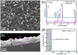
Almost all reported high-performance β-Ga2O3 films are grown by molecular beam epitaxy, metal organic chemical vapor deposition, and pulsed laser deposition at very high cost and low yield. A method for preparing micron-thick Ga2O3 films by in situ thermal oxidation of gallium without vacuum and catalysts is reported for the first time. The results show that the thickness of our typical Ga2O3 film exceeds 2 μm, the typical grain size reaches the micrometer level, and it is high-purity single-phase β-Ga2O3. The photodetector based on the thick β-Ga2O3 film has a responsivity of more than 1.7 A W−1, a light-to-dark current ratio of more than 103, a detectivity of more than 1.5 × 1013 cm Hz1/2 W−1, self-powered characteristics, and good solar-blind ultraviolet imaging properties. The potential mechanisms of high gain and self-powered characteristics of our device are analyzed. Our research results provide a method for the preparation of high-quality thick gallium oxide films and solar-blind ultraviolet photodetectors.
几乎所有已报道的高性能β-Ga2O3薄膜都是通过分子束外延、金属有机化学气相沉积和脉冲激光沉积来生长的,成本非常高,产量很低。本文首次报道了一种无真空、无催化剂的镓原位热氧化制备微米厚Ga2O3薄膜的方法。结果表明:制备的Ga2O3薄膜厚度超过2 μm,典型晶粒尺寸达到微米级,为高纯度单相β-Ga2O3薄膜;基于厚β-Ga2O3薄膜的光电探测器的响应率大于1.7 a W−1,明暗电流比大于103,探测率大于1.5 × 1013 cm Hz1/2 W−1,具有自供电特性,具有良好的日盲紫外成像性能。分析了器件实现高增益和自供电特性的潜在机理。我们的研究结果为制备高质量的氧化镓厚膜和太阳盲紫外探测器提供了一种方法。
期刊介绍:
The Journal of Materials Chemistry is divided into three distinct sections, A, B, and C, each catering to specific applications of the materials under study:
Journal of Materials Chemistry A focuses primarily on materials intended for applications in energy and sustainability.
Journal of Materials Chemistry B specializes in materials designed for applications in biology and medicine.
Journal of Materials Chemistry C is dedicated to materials suitable for applications in optical, magnetic, and electronic devices.
Example topic areas within the scope of Journal of Materials Chemistry C are listed below. This list is neither exhaustive nor exclusive.
Bioelectronics
Conductors
Detectors
Dielectrics
Displays
Ferroelectrics
Lasers
LEDs
Lighting
Liquid crystals
Memory
Metamaterials
Multiferroics
Photonics
Photovoltaics
Semiconductors
Sensors
Single molecule conductors
Spintronics
Superconductors
Thermoelectrics
Topological insulators
Transistors

 求助内容:
求助内容: 应助结果提醒方式:


