Tunneling Dielectric Thickness-Dependent Behaviors in Transistors Based on Sandwiched Small Molecule and Insulating Layer Structures
IF 5.3
2区 材料科学
Q2 MATERIALS SCIENCE, MULTIDISCIPLINARY
引用次数: 0
Abstract
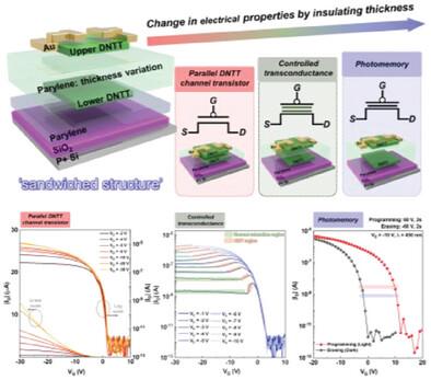
This work demonstrates the floating gate devices featuring a small molecule-insulator-small molecule-insulator sandwiched structure, where the versatile electrical characteristics can be achieved depending on the thickness of the intermediate parylene tunneling dielectric layer (TDL). For the thin parylene layer of 15 nm (parallel DNTT channel transistor), channel also forms in the lower DNTT layer, allowing hole carriers to tunnel through the parylene TDL. The parallel DNTT channel transistor exhibits electrical characteristics similar to a conventional DNTT transistor with the increased contact resistance due to the presence of the intermediate parylene layer. When the parylene TDL is slightly thicker to be 45 nm, negative differential transconductance followed by current saturation behavior is observed, due to tunneling through the parylene TDL. Finally, photomemory is demonstrated with the sufficiently thick parylene layer (≈80 nm), where hole carriers injected from the electrode cannot tunnel through the parylene TDL, allowing the lower DNTT layer to act as a floating gate for the photogenerated charge carriers. This photomemory shows programmability under the light illumination with the specific wavelength as well as the robust retention and endurance characteristics. Furthermore, the photomemory has been successfully implemented on flexible paper substrates.

基于夹层小分子和绝缘层结构的晶体管隧道介电厚度依赖行为
这项研究展示了具有小分子-绝缘体-小分子-绝缘体夹层结构的浮栅器件,根据中间对二甲苯隧穿介质层(TDL)的厚度,可以实现多种电气特性。对于 15 nm 的薄对二甲苯层(平行 DNTT 沟道晶体管),沟道也在下层 DNTT 层中形成,允许空穴载流子通过对二甲苯隧道介质层。并行 DNTT 沟道晶体管的电气特性类似于传统的 DNTT 晶体管,但由于中间对二甲苯层的存在而增加了接触电阻。当对二甲苯 TDL 稍微加厚到 45 纳米时,由于对二甲苯 TDL 的隧道效应,会出现负差分跨导,随后出现电流饱和现象。最后,在足够厚的对二甲苯层(≈80 nm)上演示了光存储,从电极注入的空穴载流子无法隧穿对二甲苯 TDL,从而使较低的 DNTT 层成为光生电荷载流子的浮动栅。这种光存储器在特定波长的光照下具有可编程性,并具有稳定的保持和耐用特性。此外,这种光存储器还成功地应用于柔性纸基板上。
本文章由计算机程序翻译,如有差异,请以英文原文为准。
求助全文
约1分钟内获得全文
求助全文
来源期刊

Advanced Electronic Materials
NANOSCIENCE & NANOTECHNOLOGYMATERIALS SCIE-MATERIALS SCIENCE, MULTIDISCIPLINARY
CiteScore
11.00
自引率
3.20%
发文量
433
期刊介绍:
Advanced Electronic Materials is an interdisciplinary forum for peer-reviewed, high-quality, high-impact research in the fields of materials science, physics, and engineering of electronic and magnetic materials. It includes research on physics and physical properties of electronic and magnetic materials, spintronics, electronics, device physics and engineering, micro- and nano-electromechanical systems, and organic electronics, in addition to fundamental research.
 求助内容:
求助内容: 应助结果提醒方式:


