Thin-Film Assisted Laser Transfer and Bonding (TFA-LTAB) for the Fabrication of Micro-LED Displays
IF 5.3
2区 材料科学
Q2 MATERIALS SCIENCE, MULTIDISCIPLINARY
引用次数: 0
Abstract
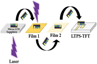
Micro-Light Emitting Diodes (Micro-LEDs) are key components in the field of next-generation display technologies. In the process of making Micro-LED displays, millions of chips need to be transferred to the driver substrate using mass transfer technology. Conventional transfer techniques, such as stamp transfer, present challenges in terms of processing efficiency and applicability due to the need for pre-prepared tethered structures and fixed chip pitch. To overcome these limitations, the t hin-film-assisted laser transfer and bonding (TFA-LTAB) technology is proposed. This technique is able to efficiently and accurately transfer Micro-LEDs from the source substrate to the driver substrate with arbitrary pitch through thin-film assistance, and electrically connects the chips through flip-chip bonding technology, which significantly improves the efficiency and reliability of the transfer and joining. The TFA-LTAB method proposed in this study integrates laser transfer and flip-chip bonding techniques. Through the TFA-LTAB process, these Micro-LEDs cultured on sapphire substrates are precisely assembled onto transparent low-temperature polycrystalline silicon thin-film transistors (LTPS-TFTs). The method successfully achieved mass transfer and bonding of Micro-LEDs with a size of 30 × 15 µm2 at low temperature (180 °C) and low pressure (0.08 MPa).
薄膜辅助激光转移和键合(TFA-LTAB)用于微型led显示器的制造
微型发光二极管(micro - led)是下一代显示技术领域的关键部件。在制造Micro-LED显示屏的过程中,需要使用传质技术将数百万个芯片转移到驱动衬底上。传统的转移技术,如印章转移,由于需要预先准备的系留结构和固定的芯片间距,在处理效率和适用性方面面临挑战。为了克服这些限制,提出了薄膜辅助激光转移键合(TFA-LTAB)技术。该技术能够通过薄膜辅助将micro - led从源基板高效、准确地转移到任意间距的驱动基板上,并通过倒装芯片键合技术将芯片电连接起来,显著提高了转移和连接的效率和可靠性。本研究提出的TFA-LTAB方法集成了激光转移和倒装芯片键合技术。通过TFA-LTAB工艺,这些培养在蓝宝石衬底上的micro - led被精确地组装在透明的低温多晶硅薄膜晶体管(ltps - tft)上。该方法在低温(180°C)和低压(0.08 MPa)下成功实现了30 × 15µm2尺寸的micro - led的传质和键合。
本文章由计算机程序翻译,如有差异,请以英文原文为准。
求助全文
约1分钟内获得全文
求助全文
来源期刊

Advanced Electronic Materials
NANOSCIENCE & NANOTECHNOLOGYMATERIALS SCIE-MATERIALS SCIENCE, MULTIDISCIPLINARY
CiteScore
11.00
自引率
3.20%
发文量
433
期刊介绍:
Advanced Electronic Materials is an interdisciplinary forum for peer-reviewed, high-quality, high-impact research in the fields of materials science, physics, and engineering of electronic and magnetic materials. It includes research on physics and physical properties of electronic and magnetic materials, spintronics, electronics, device physics and engineering, micro- and nano-electromechanical systems, and organic electronics, in addition to fundamental research.
 求助内容:
求助内容: 应助结果提醒方式:


