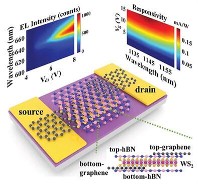
A Bifunctional Tunneling Device for Photodetection and Electroluminescence Using van der Waals Heterostructure
IF 5.3
2区 材料科学
Q2 MATERIALS SCIENCE, MULTIDISCIPLINARY
引用次数: 0
Abstract
Two-dimensional (2D) materials are widely used in various optical, electronic, and optoelectronic devices. However, the realization of visible light emission and near-infrared photodetection functions in a single device remains a challenge. Here, an integrated dual-functional device is developed by manipulating the excitons of WS2 within a graphene/hBN/WS2/graphene heterostructure. When operating as a photodetector at low external bias, the dark current is well suppressed by the hBN layer. With the excellent two-photon absorption (TPA) property of monolayer WS2, the photoresponse range of the photodetector can be extended to the near-infrared region, achieving a responsivity of up to 0.19 mA/W at 1145 nm. At high external bias, the device can work in light-emitting mode, in which the electroluminescence (EL) wavelength can be tuned via gate voltage. This atomically thin device opens up possibilities for applications in miniaturized display, sensing, and monitoring systems.

利用范德华异质结构的光探测和电致发光双功能隧道装置
二维(2D)材料广泛应用于各种光学、电子和光电子器件中。然而,在单一器件中实现可见光发射和近红外光探测功能仍然是一个挑战。本文通过在石墨烯/hBN/WS2/石墨烯异质结构中操纵WS2的激子,开发了一种集成的双功能器件。当作为光电探测器在低外偏置下工作时,暗电流被hBN层很好地抑制。利用单层WS2优异的双光子吸收(TPA)特性,光电探测器的光响应范围可扩展到近红外区域,在1145 nm处的响应率高达0.19 mA/W。在高外偏置下,该器件可以在发光模式下工作,其中电致发光(EL)波长可以通过栅极电压调谐。这种原子级薄的设备为小型化显示、传感和监控系统的应用开辟了可能性。
本文章由计算机程序翻译,如有差异,请以英文原文为准。
求助全文
约1分钟内获得全文
求助全文
来源期刊

Advanced Electronic Materials
NANOSCIENCE & NANOTECHNOLOGYMATERIALS SCIE-MATERIALS SCIENCE, MULTIDISCIPLINARY
CiteScore
11.00
自引率
3.20%
发文量
433
期刊介绍:
Advanced Electronic Materials is an interdisciplinary forum for peer-reviewed, high-quality, high-impact research in the fields of materials science, physics, and engineering of electronic and magnetic materials. It includes research on physics and physical properties of electronic and magnetic materials, spintronics, electronics, device physics and engineering, micro- and nano-electromechanical systems, and organic electronics, in addition to fundamental research.
文献相关原料
公司名称
产品信息
阿拉丁
sulfur (S)
阿拉丁
WO3
 求助内容:
求助内容: 应助结果提醒方式:


