Extension Doping with Low-Resistance Contacts for P-Type Monolayer WSe2 Field-Effect Transistors
IF 5.3
2区 材料科学
Q2 MATERIALS SCIENCE, MULTIDISCIPLINARY
引用次数: 0
Abstract
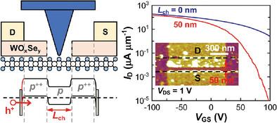
Source/Drain extension doping is crucial for minimizing the series resistance of the ungated channel and reducing the contact resistance of field-effect transistors (FETs) in complementary metal–oxide–semiconductor (CMOS) technology. 2D semiconductors, such as MoS2 and WSe2, are promising channel materials for beyond-silicon CMOS. A key challenge is to achieve extension doping for 2D monolayer FETs without damaging the atomically thin material. This work demonstrates extension doping with low-resistance contacts for monolayer WSe2 p-FETs. Self-limiting oxidation transforms a bilayer WSe2 into a hetero-bilayer of a high-work-function WOxSey on a monolayer WSe2. Then, damage-free nanolithography defines an undoped nano-channel, preserving the high on-current of WOxSey-doped FETs while significantly improving their on/off ratio. The insertion of an amorphous WOxSey interlayer under the contacts achieves record-low contact resistances for monolayer WSe2 over a hole density range of 1012 to 1013 cm−2 (1.2 ± 0.3 kΩ µm at 1013 cm−2). The WOxSey-doped extension exhibits a sheet resistance as low as 10 ± 1 kΩ □−1. Monolayer WSe2 p-FETs with sub-50 nm channel lengths reach a maximum drain current of 154 µA µm−1 with an on/off ratio of 107–108. These results define strategies for nanometer-scale selective-area doping in 2D FETs and other 2D architectures.
p型单层WSe2场效应晶体管的低阻触点延伸掺杂
在互补金属氧化物半导体(CMOS)技术中,源极/漏极扩展掺杂对于最小化非门控通道的串联电阻和降低场效应晶体管(fet)的接触电阻至关重要。二维半导体,如MoS2和WSe2,是有前途的超硅CMOS通道材料。一个关键的挑战是在不破坏原子薄材料的情况下实现二维单层场效应管的扩展掺杂。这项工作证明了单层WSe2 p- fet具有低电阻触点的扩展掺杂。自限氧化将双层WSe2转化为单层WSe2上的高工作功能WOxSey的异双分子层。然后,无损伤纳米光刻定义了一个未掺杂的纳米通道,保留了woxsey掺杂fet的高导通电流,同时显著提高了它们的导通/关断比。在触点下插入无定形WOxSey中间层,在1012至1013 cm−2的空穴密度范围内(1013 cm−2时为1.2±0.3 kΩµm),单层WSe2的接触电阻达到了创纪录的低水平。掺杂woxsey的延伸片电阻低至10±1 kΩ□−1。通道长度低于50 nm的单层WSe2 p- fet最大漏极电流为154µaµm−1,通/关比为107-108。这些结果定义了在二维场效应管和其他二维结构中纳米尺度选择性区域掺杂的策略。
本文章由计算机程序翻译,如有差异,请以英文原文为准。
求助全文
约1分钟内获得全文
求助全文
来源期刊

Advanced Electronic Materials
NANOSCIENCE & NANOTECHNOLOGYMATERIALS SCIE-MATERIALS SCIENCE, MULTIDISCIPLINARY
CiteScore
11.00
自引率
3.20%
发文量
433
期刊介绍:
Advanced Electronic Materials is an interdisciplinary forum for peer-reviewed, high-quality, high-impact research in the fields of materials science, physics, and engineering of electronic and magnetic materials. It includes research on physics and physical properties of electronic and magnetic materials, spintronics, electronics, device physics and engineering, micro- and nano-electromechanical systems, and organic electronics, in addition to fundamental research.
 求助内容:
求助内容: 应助结果提醒方式:


