Influence and mechanism of ultrafast laser-textured Cu substrate on wetting behavior of SAC305 solder
IF 4.6
2区 物理与天体物理
Q1 OPTICS
引用次数: 0
Abstract
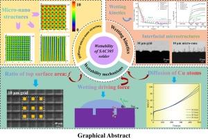
Periodic arrays of grids, micro-cones, and grooves were successfully fabricated on Cu substrate using ultrafast laser technology. The wetting behavior of SAC305 solder on micro-nano structured Cu substrates was investigated, and the influence mechanism of superficial micro-nano structure was discussed using classical wetting model and molecular dynamics (MD) simulation. The results indicate that compared to polished surface, all the superficial micro-nano structures on Cu substrate improve the wettability and wetting kinetics of SAC305 solder. Especially, grid structure shows the most significant improvement, and the effect is further enhanced with the increase of processing depth. When the processing depth of grid structure is 25 μm, the smallest wetting angle of 15.1° and wetting equilibrium time of 29 s were achieved. The wetting process of SAC305 solder on Cu substrate is composed of rapid reaction stage, stable diffusion state, and equilibrium stage. Rn ∼ t relationship curve reveals that the influence of micro-nano structure on wetting kinetics mainly occurs in the rapid reaction stage. The enhancement of wettability and wetting kinetics from superficial micro-nano structure can be attributed to the introduced extra capillary force and the improved atomic diffusion rate on the wetting interface.

超快激光纹理铜基板对 SAC305 焊料润湿行为的影响和机理
利用超快激光技术在铜基底上成功制造出了周期性的网格、微锥和凹槽阵列。利用经典润湿模型和分子动力学(MD)模拟研究了 SAC305 焊料在微纳结构铜基底上的润湿行为,并探讨了表层微纳结构的影响机理。结果表明,与抛光表面相比,铜基底上的所有表层微纳结构都能改善 SAC305 焊料的润湿性和润湿动力学。尤其是栅格结构的改善效果最为显著,而且随着加工深度的增加,效果会进一步增强。当网格结构的加工深度为 25 μm 时,达到的最小润湿角为 15.1°,润湿平衡时间为 29 s。SAC305 焊料在铜基板上的润湿过程由快速反应阶段、稳定扩散状态和平衡阶段组成。Rn ∼ t 关系曲线表明,微纳结构对润湿动力学的影响主要发生在快速反应阶段。表层微纳结构对润湿性和润湿动力学的增强可归因于润湿界面上引入的额外毛细管力和原子扩散速率的提高。
本文章由计算机程序翻译,如有差异,请以英文原文为准。
求助全文
约1分钟内获得全文
求助全文
来源期刊
CiteScore
8.50
自引率
10.00%
发文量
1060
审稿时长
3.4 months
期刊介绍:
Optics & Laser Technology aims to provide a vehicle for the publication of a broad range of high quality research and review papers in those fields of scientific and engineering research appertaining to the development and application of the technology of optics and lasers. Papers describing original work in these areas are submitted to rigorous refereeing prior to acceptance for publication.
The scope of Optics & Laser Technology encompasses, but is not restricted to, the following areas:
•development in all types of lasers
•developments in optoelectronic devices and photonics
•developments in new photonics and optical concepts
•developments in conventional optics, optical instruments and components
•techniques of optical metrology, including interferometry and optical fibre sensors
•LIDAR and other non-contact optical measurement techniques, including optical methods in heat and fluid flow
•applications of lasers to materials processing, optical NDT display (including holography) and optical communication
•research and development in the field of laser safety including studies of hazards resulting from the applications of lasers (laser safety, hazards of laser fume)
•developments in optical computing and optical information processing
•developments in new optical materials
•developments in new optical characterization methods and techniques
•developments in quantum optics
•developments in light assisted micro and nanofabrication methods and techniques
•developments in nanophotonics and biophotonics
•developments in imaging processing and systems

 求助内容:
求助内容: 应助结果提醒方式:


