Atomic imprint crystallization: Externally-templated crystallization of amorphous silicon
IF 10
2区 材料科学
Q1 MATERIALS SCIENCE, MULTIDISCIPLINARY
引用次数: 0
Abstract
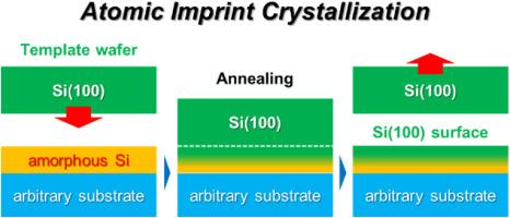
In this paper, we demonstrate the crystallization of an amorphous Si layer via atomic imprint crystallization (AIC), where an amorphous Si layer is crystallized by solid phase epitaxy (SPE) from an externally impressed single-crystal Si template that is then peeled off via delamination following crystallization. Microstructural analysis using electron backscattered diffraction (EBSD) and transmission electron microscopy (TEM) studies of the delaminated (crystallized) films reveals that the top surface of the amorphous Si layer is crystallized by SPE with regions (up to ∼5 mm diameter) composed of epitaxial domains (lateral size of few μm), all of which bear the same crystalline orientation as that of the template crystal. Unlike conventional SPE, the crystallization is not uniform across the entire region: the grains contain crystal defects such as dislocations, stacking faults, and twins; and while the crystallization is initiated at the top surface of the film, the thickness of the single-crystalline area is limited to ∼40 nm from the top surface. Clearly, the AIC approach leads to SPE (aligned with the template's crystalline orientation) over areas as large as few mms, but the crystallization is defective and incomplete through the film. We attribute this to be a consequence of the tensile stress field created at the amorphous/crystalline frontline by the volume change of amorphous Si during the crystallization. Our results establish the feasibility of imprint crystallization, and points to the direction of a new process that may enable the creation of single crystal pockets in integrated device stacks in a scalable fashion without the need for an underlying single crystal substrate. However, our results also indicate that the crystallization is of a poor quality and indicates the need for further optimization of the crystallization method.

原子印迹结晶:非晶硅的外部诱导结晶
在本文中,我们展示了通过原子印记结晶 (AIC) 实现非晶硅层结晶的过程,即通过固相外延 (SPE) 从外部印记单晶硅模板上结晶出非晶硅层,然后在结晶后通过分层剥离非晶硅层。利用电子反向散射衍射 (EBSD) 和透射电子显微镜 (TEM) 对分层(结晶)薄膜进行的微观结构分析表明,非晶态硅层的顶面是通过 SPE 结晶而成的,结晶区域(直径可达 5 毫米)由外延畴组成(横向尺寸为几微米),所有这些畴都具有与模板晶体相同的结晶取向。与传统的 SPE 不同,整个区域的结晶并不均匀:晶粒含有晶体缺陷,如位错、堆叠断层和孪晶;虽然结晶是在薄膜的顶面开始的,但单晶区域的厚度仅限于距顶面 40 纳米。显然,AIC 方法可在几毫米大的区域内产生 SPE(与模板的结晶取向一致),但整个薄膜的结晶是有缺陷和不完整的。我们认为这是结晶过程中无定形硅的体积变化在无定形/结晶前线产生拉应力场的结果。我们的研究结果证明了压印结晶的可行性,并指明了新工艺的方向,即无需底层单晶衬底,就能以可扩展的方式在集成器件堆栈中创建单晶口袋。不过,我们的研究结果也表明,结晶质量不高,需要进一步优化结晶方法。
本文章由计算机程序翻译,如有差异,请以英文原文为准。
求助全文
约1分钟内获得全文
求助全文
来源期刊
Materials Today Physics
Materials Science-General Materials Science
CiteScore
14.00
自引率
7.80%
发文量
284
审稿时长
15 days
期刊介绍:
Materials Today Physics is a multi-disciplinary journal focused on the physics of materials, encompassing both the physical properties and materials synthesis. Operating at the interface of physics and materials science, this journal covers one of the largest and most dynamic fields within physical science. The forefront research in materials physics is driving advancements in new materials, uncovering new physics, and fostering novel applications at an unprecedented pace.
 求助内容:
求助内容: 应助结果提醒方式:


