Characterization of machined surface in semi-conductive SiC wafer subjected to micro-EDM drilling
IF 4.2
3区 工程技术
Q2 ENGINEERING, ELECTRICAL & ELECTRONIC
引用次数: 0
Abstract
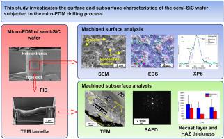
Semi-conductive silicon carbide (semi-SiC) wafers are essential in the semiconductor industry, but their high hardness and brittleness make traditional machining difficult. Electric discharge machining (EDM) is an alternative method for machining semi-SiC wafer. This study investigates the effects of discharge energy parameters, such as pulse-on time and peak current, on the surface and subsurface characteristics of semi-SiC wafers subjected to micro-EDM drilling. The machined surface and subsurface morphology and microstructure were characterized using scanning electron microscopy (SEM), energy dispersive X-ray spectroscopy (EDS), X-ray photoelectron spectroscopy (XPS), and transmission electron microscopy (TEM). SEM micrographs revealed the presence of craters, resolidified material, cracks, and micro-pores on the machined surface, influenced by the thermal energy generated during the EDM process. The material removal mechanisms identified include melting, vaporization, spalling, and oxidation. EDS analyses indicated a larger discharge energy led to an increase in carbon and oxygen concentrations on the machined surfaces, likely due to the decomposition of SiC and oxidation during EDM. XPS analysis identified the presence of graphite, SiO2, Cu particles, Cu2O, and CuO on the machined surface. TEM micrographs revealed three distinct regions in the subsurface, namely a recast layer, a heat-affected zone (HAZ), and the unaffected bulk SiC. These layers exhibited different microstructures, with the thickness of the recast layer and HAZ being dependent on the discharge energy. This study highlights the advantages of micro-EDM over other techniques, achieving a thin recast layer and minimal HAZ, thereby preserving the surface and subsurface integrity of the semi-SiC wafer.

微电火花钻孔加工半导电碳化硅晶片表面的特征
半导电碳化硅(semi-SiC)晶片是半导体工业中不可或缺的材料,但由于其硬度高、脆性大,传统的加工方法很难加工。放电加工(EDM)是加工半碳化硅晶片的一种替代方法。本研究探讨了脉冲接通时间和峰值电流等放电能量参数对微电火花钻孔加工半 SiC 晶圆表面和亚表面特性的影响。使用扫描电子显微镜 (SEM)、能量色散 X 射线光谱 (EDS)、X 射线光电子能谱 (XPS) 和透射电子显微镜 (TEM) 对加工表面和次表面形态及微观结构进行了表征。扫描电镜显微照片显示,受电火花加工过程中产生的热能影响,加工表面出现了凹坑、分解材料、裂纹和微孔。材料去除机制包括熔化、汽化、剥落和氧化。EDS 分析表明,放电能量越大,加工表面的碳和氧浓度就越高,这可能是由于电火花加工过程中碳化硅的分解和氧化作用造成的。XPS 分析确定了加工表面存在石墨、SiO2、铜颗粒、Cu2O 和 CuO。TEM 显微照片显示了次表面的三个不同区域,即再铸层、热影响区 (HAZ) 和未受影响的整体 SiC。这些层表现出不同的微观结构,重铸层和热影响区的厚度取决于放电能量。与其他技术相比,这项研究凸显了微型放电加工的优势,即可以获得较薄的再铸层和最小的热影响区,从而保持半碳化硅晶片表面和次表面的完整性。
本文章由计算机程序翻译,如有差异,请以英文原文为准。
求助全文
约1分钟内获得全文
求助全文
来源期刊

Materials Science in Semiconductor Processing
工程技术-材料科学:综合
CiteScore
8.00
自引率
4.90%
发文量
780
审稿时长
42 days
期刊介绍:
Materials Science in Semiconductor Processing provides a unique forum for the discussion of novel processing, applications and theoretical studies of functional materials and devices for (opto)electronics, sensors, detectors, biotechnology and green energy.
Each issue will aim to provide a snapshot of current insights, new achievements, breakthroughs and future trends in such diverse fields as microelectronics, energy conversion and storage, communications, biotechnology, (photo)catalysis, nano- and thin-film technology, hybrid and composite materials, chemical processing, vapor-phase deposition, device fabrication, and modelling, which are the backbone of advanced semiconductor processing and applications.
Coverage will include: advanced lithography for submicron devices; etching and related topics; ion implantation; damage evolution and related issues; plasma and thermal CVD; rapid thermal processing; advanced metallization and interconnect schemes; thin dielectric layers, oxidation; sol-gel processing; chemical bath and (electro)chemical deposition; compound semiconductor processing; new non-oxide materials and their applications; (macro)molecular and hybrid materials; molecular dynamics, ab-initio methods, Monte Carlo, etc.; new materials and processes for discrete and integrated circuits; magnetic materials and spintronics; heterostructures and quantum devices; engineering of the electrical and optical properties of semiconductors; crystal growth mechanisms; reliability, defect density, intrinsic impurities and defects.
 求助内容:
求助内容: 应助结果提醒方式:


