Jian-Sian Li, Chiao-Ching Chiang, Hsiao-Hsuan Wan, Madani Labed, Jang Hyeok Park, You Seung Rim, Meng-Hsun Yu, Fan Ren, Yu-Te Liao and Stephen J. Pearton
{"title":"Hybrid Schottky and heterojunction vertical β-Ga2O3 rectifiers†","authors":"Jian-Sian Li, Chiao-Ching Chiang, Hsiao-Hsuan Wan, Madani Labed, Jang Hyeok Park, You Seung Rim, Meng-Hsun Yu, Fan Ren, Yu-Te Liao and Stephen J. Pearton","doi":"10.1039/D4TC03046J","DOIUrl":null,"url":null,"abstract":"<p >Junction barrier Schottky design Ga<small><sub>2</sub></small>O<small><sub>3</sub></small> rectifiers allow for a combination of low turn-on voltage and high breakdown voltage. Ni/Au/Ga<small><sub>2</sub></small>O<small><sub>3</sub></small> Schottky rectifiers and NiO/Ga<small><sub>2</sub></small>O<small><sub>3</sub></small> heterojunction rectifiers were fabricated on the same wafer and the percentage of the relative areas and diameters of each were varied from pure Schottky devices to pure heterojunction devices. The on-voltage increased from 0.6 V for Schottky rectifiers to 2.4 V for heterojunction rectifiers, with a monotonic decrease in forward current at fixed bias of 5 V from 375 nA cm<small><sup>−2</sup></small> to 175 nA cm<small><sup>−2</sup></small>. Conversely, the breakdown voltage increased monotonically as the proportion of heterojunction area increased, from 1.2 kV for Schottky rectifiers to 6.2 kV for pure heterojunction devices. Breakdown mostly was initiated at the edge of the anode contact but could also occur at the transition region from the Schottky contact to NiO edge termination. The Baliga figure of merit increased with both the relative percentage of area and diameter of the heterojunction contact from 0.2 GW cm<small><sup>−2</sup></small> to 3 GW cm<small><sup>−2</sup></small>, while the energy loss during switching also increased from 2 to 3.9 W cm<small><sup>−2</sup></small>. These trends illustrate the trade-offs of Schottky <em>versus</em> pn junctions for the operation of Ga<small><sub>2</sub></small>O<small><sub>3</sub></small> rectifiers.</p>","PeriodicalId":84,"journal":{"name":"Journal of Materials Chemistry C","volume":" 43","pages":" 17563-17573"},"PeriodicalIF":5.7000,"publicationDate":"2024-09-24","publicationTypes":"Journal Article","fieldsOfStudy":null,"isOpenAccess":false,"openAccessPdf":"","citationCount":"0","resultStr":null,"platform":"Semanticscholar","paperid":null,"PeriodicalName":"Journal of Materials Chemistry C","FirstCategoryId":"1","ListUrlMain":"https://pubs.rsc.org/en/content/articlelanding/2024/tc/d4tc03046j","RegionNum":2,"RegionCategory":"材料科学","ArticlePicture":[],"TitleCN":null,"AbstractTextCN":null,"PMCID":null,"EPubDate":"","PubModel":"","JCR":"Q2","JCRName":"MATERIALS SCIENCE, MULTIDISCIPLINARY","Score":null,"Total":0}
引用次数: 0
Abstract
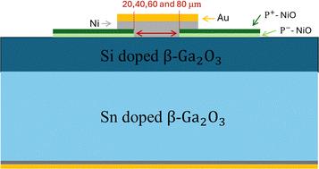
Junction barrier Schottky design Ga2O3 rectifiers allow for a combination of low turn-on voltage and high breakdown voltage. Ni/Au/Ga2O3 Schottky rectifiers and NiO/Ga2O3 heterojunction rectifiers were fabricated on the same wafer and the percentage of the relative areas and diameters of each were varied from pure Schottky devices to pure heterojunction devices. The on-voltage increased from 0.6 V for Schottky rectifiers to 2.4 V for heterojunction rectifiers, with a monotonic decrease in forward current at fixed bias of 5 V from 375 nA cm−2 to 175 nA cm−2. Conversely, the breakdown voltage increased monotonically as the proportion of heterojunction area increased, from 1.2 kV for Schottky rectifiers to 6.2 kV for pure heterojunction devices. Breakdown mostly was initiated at the edge of the anode contact but could also occur at the transition region from the Schottky contact to NiO edge termination. The Baliga figure of merit increased with both the relative percentage of area and diameter of the heterojunction contact from 0.2 GW cm−2 to 3 GW cm−2, while the energy loss during switching also increased from 2 to 3.9 W cm−2. These trends illustrate the trade-offs of Schottky versus pn junctions for the operation of Ga2O3 rectifiers.
期刊介绍:
The Journal of Materials Chemistry is divided into three distinct sections, A, B, and C, each catering to specific applications of the materials under study:
Journal of Materials Chemistry A focuses primarily on materials intended for applications in energy and sustainability.
Journal of Materials Chemistry B specializes in materials designed for applications in biology and medicine.
Journal of Materials Chemistry C is dedicated to materials suitable for applications in optical, magnetic, and electronic devices.
Example topic areas within the scope of Journal of Materials Chemistry C are listed below. This list is neither exhaustive nor exclusive.
Bioelectronics
Conductors
Detectors
Dielectrics
Displays
Ferroelectrics
Lasers
LEDs
Lighting
Liquid crystals
Memory
Metamaterials
Multiferroics
Photonics
Photovoltaics
Semiconductors
Sensors
Single molecule conductors
Spintronics
Superconductors
Thermoelectrics
Topological insulators
Transistors

 求助内容:
求助内容: 应助结果提醒方式:


