Semiconductor WO3 thin films deposited by pulsed reactive magnetron sputtering
IF 4.2
3区 工程技术
Q2 ENGINEERING, ELECTRICAL & ELECTRONIC
引用次数: 0
Abstract
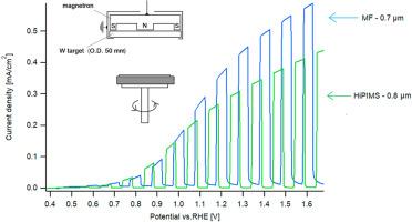
A pulsed reactive magnetron sputtering system with a tungsten target and a gas mixture of argon and oxygen was investigated as a source for the deposition of semiconductor WO3 thin films on soda lime glass substrates and on the glass with transparent conductive SnO2:F (FTO) electrode. The reactive sputtering process was performed in HiPIMS mode with low pulse repetition frequency fp ≈ 50–100 Hz and short pulse duration in HiPIMS discharge Ton = 100 μs. The second mode investigated was the mid-frequency (MF) magnetron discharge with pulse frequency fp = 40 kHz and pulse length Ton = 15 μs. The plasma parameters were investigated for both HiPIMS and MF modes using the planar RF probe operating at the frequency fprobe = 350 kHz and the grid QCM with biased collector electrode. Ion density ni and tail electron temperature (Te) were determined in both pulsed reactive magnetron sputtering discharge modes with time resolution. The maximum value ni ≈ 5 · 1017 m−3 was found in the reactive HiPIMS mode, and the maximum value ni ≈ 7 · 1016 m−3 was found in the reactive MF (40 kHz) mode. The degree of ionization of sputtered particles in reactive HiPIMS was determined for different values of (QO2) and was found to be in the range of ri ≈ 0.1–0.3. The deposition rate determined by QCM in reactive HiPIMS was practically independent on (QO2), but in the case of reactive MF, the measured deposition rate decreased significantly with increasing (QO2). The WO3 films deposited in both modes have a predominantly monoclinic crystal structure. The light and dark conductivity and the light/dark conductivity ratio (Ld) were measured under dark conditions and UV light illumination. At higher (QO2), the maximum value of Ld ≈ 300 was found for MF deposited WO3 and the maximum value of Ld ≈ 30 was found for HiPIMS deposited WO3. The photoelectrochemical measurement of WO3 deposited on FTO electrodes confirmed the n-type conductivity, and these films functioned as photoanodes in photoelectrochemical cells. MF deposited WO3 films systematically exhibited slightly higher photocurrents than HiPIMS deposited WO3. It was shown that these optimum photocurrents for HiPIMS and MF were found at QO2 ≈ 80 sccm and could not be improved by further increasing of (QO2).

通过脉冲反应磁控溅射沉积的半导体 WO3 薄膜
研究了一种脉冲反应磁控溅射系统,该系统采用钨靶和氩氧混合气体作为源,用于在钠钙玻璃基片和带有透明导电 SnO2:F (FTO) 电极的玻璃上沉积半导体 WO3 薄膜。反应溅射过程在 HiPIMS 模式下进行,低脉冲重复频率 fp ≈ 50-100 Hz,HiPIMS 放电 Ton = 100 μs 脉冲持续时间短。研究的第二种模式是中频(MF)磁控管放电,脉冲频率 fp = 40 kHz,脉冲长度 Ton = 15 μs。利用频率为 fprobe = 350 kHz 的平面射频探头和带有偏置集电极的栅格 QCM,对 HiPIMS 和 MF 模式的等离子体参数进行了研究。两种脉冲反应磁控溅射放电模式下的离子密度 ni 和尾电子温度 (Te) 都是以时间分辨率测定的。在反应式 HiPIMS 模式下,最大值 ni ≈ 5 - 1017 m-3,而在反应式 MF(40 kHz)模式下,最大值 ni ≈ 7 - 1016 m-3。针对不同的 (QO2) 值,测定了反应式 HiPIMS 中溅射粒子的电离度,发现其范围为 ri ≈ 0.1-0.3。在反应式 HiPIMS 中,QCM 测定的沉积速率实际上与 (QO2) 无关,但在反应式 MF 中,随着 (QO2) 的增加,测得的沉积速率显著下降。在这两种模式下沉积的 WO3 薄膜主要具有单斜晶体结构。在黑暗条件和紫外光照射下测量了光导率、暗导率以及光/暗导率比 (Ld)。在较高(QO2)的条件下,发现 MF 沉积的 WO3 的最大值 Ld ≈ 300,而 HiPIMS 沉积的 WO3 的最大值 Ld ≈ 30。对沉积在 FTO 电极上的 WO3 进行的光电化学测量证实了其 n 型导电性,这些薄膜可用作光电化学电池中的光阳极。MF 沉积的 WO3 薄膜系统地显示出比 HiPIMS 沉积的 WO3 稍高的光电流。研究表明,HiPIMS 和 MF 的最佳光电流出现在 QO2 ≈ 80 sccm 时,并且不能通过进一步增加 (QO2) 来提高。
本文章由计算机程序翻译,如有差异,请以英文原文为准。
求助全文
约1分钟内获得全文
求助全文
来源期刊

Materials Science in Semiconductor Processing
工程技术-材料科学:综合
CiteScore
8.00
自引率
4.90%
发文量
780
审稿时长
42 days
期刊介绍:
Materials Science in Semiconductor Processing provides a unique forum for the discussion of novel processing, applications and theoretical studies of functional materials and devices for (opto)electronics, sensors, detectors, biotechnology and green energy.
Each issue will aim to provide a snapshot of current insights, new achievements, breakthroughs and future trends in such diverse fields as microelectronics, energy conversion and storage, communications, biotechnology, (photo)catalysis, nano- and thin-film technology, hybrid and composite materials, chemical processing, vapor-phase deposition, device fabrication, and modelling, which are the backbone of advanced semiconductor processing and applications.
Coverage will include: advanced lithography for submicron devices; etching and related topics; ion implantation; damage evolution and related issues; plasma and thermal CVD; rapid thermal processing; advanced metallization and interconnect schemes; thin dielectric layers, oxidation; sol-gel processing; chemical bath and (electro)chemical deposition; compound semiconductor processing; new non-oxide materials and their applications; (macro)molecular and hybrid materials; molecular dynamics, ab-initio methods, Monte Carlo, etc.; new materials and processes for discrete and integrated circuits; magnetic materials and spintronics; heterostructures and quantum devices; engineering of the electrical and optical properties of semiconductors; crystal growth mechanisms; reliability, defect density, intrinsic impurities and defects.
 求助内容:
求助内容: 应助结果提醒方式:


