A review: CNT/diamond composites prepared via CVD and its potential applications
IF 4.2
3区 工程技术
Q2 ENGINEERING, ELECTRICAL & ELECTRONIC
引用次数: 0
Abstract
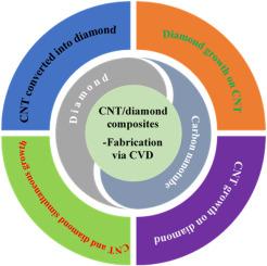
As the demand for semiconductor preparation technology continues to grow in society and the miniaturization of silicon-based semiconductors is approaching physical limits, it is necessary to search for suitable materials as alternatives for nanoscale devices and technologies. Carbon nanotube/diamond (CNT/diamond) composites, a combination of post-Moore era and ultimate semiconductor materials, combine unique one-dimensional and three-dimensional structures of carbon materials with excellent thermal, mechanical, and electrical properties and have the potential to develop into a new generation of high heat flux management devices and new semiconductor devices. In the past 15 years, there were many studies focusing on the integration of diamond with CNT, while it is still a challenge to maximum fulfill all the advantage of both materials. In this review, recent research progresses on the synthesis of CNT/diamond composites by the chemical vapor deposition (CVD) method are analyzed, including the formation of the CNT/diamond interface, and the application of CNT/diamond composites. The CVD methods for preparing CNT/diamond composites, as well as the various shapes and interface characteristics of CNT/diamond composites, are all thoroughly discussed. And guidelines are provided for various composite application scenarios. Finally, the challenges of the interface characteristics of CNT/diamond composites produced by CVD method are summarized. It is believed that CNT/diamond has great potentials in thermal management and semiconductor devices in the future.

综述:通过 CVD 制备的 CNT/金刚石复合材料及其潜在应用
随着社会对半导体制备技术的需求不断增长,硅基半导体的微型化已接近物理极限,因此有必要寻找合适的材料作为纳米级器件和技术的替代品。碳纳米管/金刚石(CNT/diamond)复合材料是后摩尔时代与终极半导体材料的结合,它结合了碳材料独特的一维和三维结构,具有优异的热学、机械和电学特性,有望发展成为新一代高热通量管理器件和新型半导体器件。在过去的 15 年中,有许多研究关注金刚石与碳纳米管的结合,但如何最大限度地发挥两种材料的所有优势仍是一个挑战。本综述分析了近年来利用化学气相沉积(CVD)方法合成 CNT/金刚石复合材料的研究进展,包括 CNT/金刚石界面的形成以及 CNT/金刚石复合材料的应用。对制备碳纳米管/金刚石复合材料的 CVD 方法以及碳纳米管/金刚石复合材料的各种形状和界面特征进行了深入讨论。并为各种复合材料的应用场景提供了指导。最后,总结了 CVD 法生产的 CNT/金刚石复合材料界面特性所面临的挑战。相信未来 CNT/金刚石在热管理和半导体器件方面具有巨大潜力。
本文章由计算机程序翻译,如有差异,请以英文原文为准。
求助全文
约1分钟内获得全文
求助全文
来源期刊

Materials Science in Semiconductor Processing
工程技术-材料科学:综合
CiteScore
8.00
自引率
4.90%
发文量
780
审稿时长
42 days
期刊介绍:
Materials Science in Semiconductor Processing provides a unique forum for the discussion of novel processing, applications and theoretical studies of functional materials and devices for (opto)electronics, sensors, detectors, biotechnology and green energy.
Each issue will aim to provide a snapshot of current insights, new achievements, breakthroughs and future trends in such diverse fields as microelectronics, energy conversion and storage, communications, biotechnology, (photo)catalysis, nano- and thin-film technology, hybrid and composite materials, chemical processing, vapor-phase deposition, device fabrication, and modelling, which are the backbone of advanced semiconductor processing and applications.
Coverage will include: advanced lithography for submicron devices; etching and related topics; ion implantation; damage evolution and related issues; plasma and thermal CVD; rapid thermal processing; advanced metallization and interconnect schemes; thin dielectric layers, oxidation; sol-gel processing; chemical bath and (electro)chemical deposition; compound semiconductor processing; new non-oxide materials and their applications; (macro)molecular and hybrid materials; molecular dynamics, ab-initio methods, Monte Carlo, etc.; new materials and processes for discrete and integrated circuits; magnetic materials and spintronics; heterostructures and quantum devices; engineering of the electrical and optical properties of semiconductors; crystal growth mechanisms; reliability, defect density, intrinsic impurities and defects.
 求助内容:
求助内容: 应助结果提醒方式:


