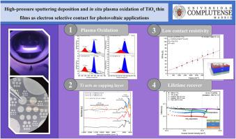
High-pressure sputtering deposition and in situ plasma oxidation of TiOx thin films as electron selective contact for photovoltaic applications
IF 4.6
3区 工程技术
Q2 ENGINEERING, ELECTRICAL & ELECTRONIC
引用次数: 0
Abstract
In this article, we show the structural, optical, and electrical characterization of TiOx deposited by the unconventional technique of High-Pressure Sputtering (HPS). This technique has the potential to reduce the plasma-induced damage of the samples. To fabricate the TiOx, a 2-step process was used. Firstly, a thin Ti film was deposited in an Ar atmosphere. Secondly, O2 was introduced into the HPS chamber to create an Ar/O2 plasma that, along with low temperatures (150 °C or 200 °C), induces the oxidation of the deposited Ti film. With this approach, the Ti film is expected to behave as a capping layer that will reduce the oxidation of the Si substrate. This study aims to obtain a TiOx layer with low specific contact resistivity (ρc) and high minority carrier lifetime. These are crucial characteristics for obtaining high-quality selective contact. It was found that the 2-step process can oxidize the Ti layer. These HPS TiOx layers show a resistivity in the order of 0.3–10 Ωcm and a ratio Ti/O of ∼1.9. Moreover, the SiOx regrowth is minimal since this is comparable to the native oxide. This was confirmed by transmission electron microscopy (TEM) and Fourier transform infrared spectroscopy (FTIR). The samples fabricated with a Ti layer (∼4 nm) plus an oxidation temperature of 200 °C (duration of less than 2 h) show a low ρc of 0.02 Ωcm2, an excellent transmittance (>87 %) in the visible region and an optical bandgap of 2.8 eV. These TiOx layers are amorphous, although some anatase phase crystalline clusters appear for the 200 °C processes. However, the minority carrier lifetime results of Si passivated by TiOx were inadequate for fabricating efficient solar cells. We also found that using the RCA oxide improved lifetime. This indicates that introducing alternative low-temperature passivating layers can solve this issue.

高压溅射沉积和原位等离子氧化氧化 TiOx 薄膜作为光伏应用的电子选择性触点
在本文中,我们展示了通过高压溅射(HPS)这一非常规技术沉积的氧化钛的结构、光学和电学特性。这种技术有可能减少等离子体对样品造成的损坏。为了制造氧化钛,采用了两步工艺。首先,在氩气环境中沉积钛薄膜。其次,将 O2 引入 HPS 室以产生 Ar/O2 等离子体,该等离子体与低温(150 ℃ 或 200 ℃)一起诱导沉积的 Ti 薄膜氧化。通过这种方法,钛薄膜有望成为一个封盖层,减少硅基底的氧化。本研究旨在获得具有低特定接触电阻率(ρc)和高少数载流子寿命的氧化钛层。这些都是获得高质量选择性接触的关键特性。研究发现,两步工艺可以氧化钛层。这些 HPS TiOx 层的电阻率为 0.3-10 Ωcm,Ti/O 比为 1.9。此外,SiOx 的再生极少,因为这与原生氧化物相当。透射电子显微镜(TEM)和傅立叶变换红外光谱(FTIR)证实了这一点。使用钛层(4 纳米)和 200 °C 的氧化温度(持续时间少于 2 小时)制作的样品显示出 0.02 Ωcm2 的低 ρc,在可见光区域具有出色的透射率(87%)和 2.8 eV 的光带隙。这些氧化钛层是无定形的,尽管在 200 °C 过程中出现了一些锐钛矿相晶簇。然而,钛氧化物钝化硅的少数载流子寿命结果不足以制造高效太阳能电池。我们还发现,使用 RCA 氧化物可提高寿命。这表明,引入其他低温钝化层可以解决这一问题。
本文章由计算机程序翻译,如有差异,请以英文原文为准。
求助全文
约1分钟内获得全文
求助全文
来源期刊

Materials Science in Semiconductor Processing
工程技术-材料科学:综合
CiteScore
8.00
自引率
4.90%
发文量
780
审稿时长
42 days
期刊介绍:
Materials Science in Semiconductor Processing provides a unique forum for the discussion of novel processing, applications and theoretical studies of functional materials and devices for (opto)electronics, sensors, detectors, biotechnology and green energy.
Each issue will aim to provide a snapshot of current insights, new achievements, breakthroughs and future trends in such diverse fields as microelectronics, energy conversion and storage, communications, biotechnology, (photo)catalysis, nano- and thin-film technology, hybrid and composite materials, chemical processing, vapor-phase deposition, device fabrication, and modelling, which are the backbone of advanced semiconductor processing and applications.
Coverage will include: advanced lithography for submicron devices; etching and related topics; ion implantation; damage evolution and related issues; plasma and thermal CVD; rapid thermal processing; advanced metallization and interconnect schemes; thin dielectric layers, oxidation; sol-gel processing; chemical bath and (electro)chemical deposition; compound semiconductor processing; new non-oxide materials and their applications; (macro)molecular and hybrid materials; molecular dynamics, ab-initio methods, Monte Carlo, etc.; new materials and processes for discrete and integrated circuits; magnetic materials and spintronics; heterostructures and quantum devices; engineering of the electrical and optical properties of semiconductors; crystal growth mechanisms; reliability, defect density, intrinsic impurities and defects.
 求助内容:
求助内容: 应助结果提醒方式:


