Copper Paste Printed Paper-Based Dual-Band Antenna for Wearable Wireless Electronics

IF 5.3 2区 材料科学 Q2 MATERIALS SCIENCE, MULTIDISCIPLINARY
Wendong Yang, Xun Zhao, Jingchang Nan, Michael Hengge, Emil J. W. List-Kratochvil
{"title":"Copper Paste Printed Paper-Based Dual-Band Antenna for Wearable Wireless Electronics","authors":"Wendong Yang, Xun Zhao, Jingchang Nan, Michael Hengge, Emil J. W. List-Kratochvil","doi":"10.1002/aelm.202400522","DOIUrl":null,"url":null,"abstract":"Wearable wireless electronics is becoming a significant research area because of the unique features of this technology. Within this field printed antennas are the key electrical component accomplishing the signal transmission and energy harvesting tasks and at the same these antennas need to be lightweight, environmentally friendly, safe to wear, and easy to conform. Currently, the majority of available paper-based antennas are designed for RFID, sensing, UWB, WLAN, and medical applications, with just a few being utilized in wearable applications, particularly for wireless body area network (WBAN). Furthermore, few studies have been conducted on the usage of printable copper conductive materials and low-temperature plasma technique for the fabrication of such antennas. This study demonstrates the realization of a dual-band paper-based wearable antenna by screen-printing of a plasma-sintered conductive copper paste. The copper paste, composed of 51 wt% solid particles, can easily produce desired conductive patterns on photo paper after printing and a subsequent plasma sintering, with a good adhesion. The antenna designed on photopaper operates in the frequency bands of 1.73–2.55 GHz and 7.66–8.89 GHz. Free-space simulation and measurement results reveal that the antenna exhibits stable radiation performance in the targeted WBAN (2.4–2.4835 GHz) and X uplink (7.9–8.4 GHz) frequency bands, together with low profile, excellent conformality and acceptable SAR values on the body and no electronic waste formed after disposal, making it a competitive candidate for usage in wearable wireless electronics.","PeriodicalId":110,"journal":{"name":"Advanced Electronic Materials","volume":"134 1","pages":""},"PeriodicalIF":5.3000,"publicationDate":"2024-10-25","publicationTypes":"Journal Article","fieldsOfStudy":null,"isOpenAccess":false,"openAccessPdf":"","citationCount":"0","resultStr":null,"platform":"Semanticscholar","paperid":null,"PeriodicalName":"Advanced Electronic Materials","FirstCategoryId":"88","ListUrlMain":"https://doi.org/10.1002/aelm.202400522","RegionNum":2,"RegionCategory":"材料科学","ArticlePicture":[],"TitleCN":null,"AbstractTextCN":null,"PMCID":null,"EPubDate":"","PubModel":"","JCR":"Q2","JCRName":"MATERIALS SCIENCE, MULTIDISCIPLINARY","Score":null,"Total":0}
引用次数: 0

Abstract

Wearable wireless electronics is becoming a significant research area because of the unique features of this technology. Within this field printed antennas are the key electrical component accomplishing the signal transmission and energy harvesting tasks and at the same these antennas need to be lightweight, environmentally friendly, safe to wear, and easy to conform. Currently, the majority of available paper-based antennas are designed for RFID, sensing, UWB, WLAN, and medical applications, with just a few being utilized in wearable applications, particularly for wireless body area network (WBAN). Furthermore, few studies have been conducted on the usage of printable copper conductive materials and low-temperature plasma technique for the fabrication of such antennas. This study demonstrates the realization of a dual-band paper-based wearable antenna by screen-printing of a plasma-sintered conductive copper paste. The copper paste, composed of 51 wt% solid particles, can easily produce desired conductive patterns on photo paper after printing and a subsequent plasma sintering, with a good adhesion. The antenna designed on photopaper operates in the frequency bands of 1.73–2.55 GHz and 7.66–8.89 GHz. Free-space simulation and measurement results reveal that the antenna exhibits stable radiation performance in the targeted WBAN (2.4–2.4835 GHz) and X uplink (7.9–8.4 GHz) frequency bands, together with low profile, excellent conformality and acceptable SAR values on the body and no electronic waste formed after disposal, making it a competitive candidate for usage in wearable wireless electronics.
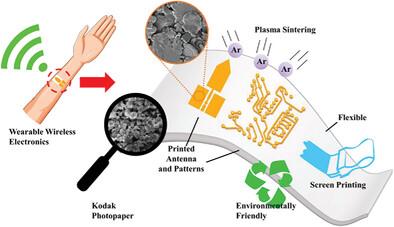
Abstract Image

用于可穿戴无线电子设备的铜浆印刷纸基双频天线
由于可穿戴无线电子技术的独特性,它正成为一个重要的研究领域。在这一领域中,印刷天线是完成信号传输和能量收集任务的关键电子元件,同时这些天线还需要重量轻、环保、佩戴安全和易于安装。目前,大多数纸基天线都是为射频识别(RFID)、传感、UWB、无线局域网和医疗应用而设计的,只有少数用于可穿戴应用,特别是无线体域网(WBAN)。此外,关于使用可印刷铜导电材料和低温等离子体技术制造此类天线的研究很少。本研究展示了通过丝网印刷等离子烧结导电铜浆实现的双频纸基可穿戴天线。这种铜浆由 51 wt% 的固体颗粒组成,经过印刷和随后的等离子烧结后,可以在相纸上轻松生成所需的导电图案,并具有良好的附着力。在相纸上设计的天线工作频段为 1.73-2.55 GHz 和 7.66-8.89 GHz。自由空间仿真和测量结果表明,该天线在目标 WBAN(2.4-2.4835 GHz)和 X 上行链路(7.9-8.4 GHz)频段具有稳定的辐射性能,而且外形小巧,与人体吻合度高,SAR 值可接受,弃置后不会产生电子废物,是可穿戴无线电子产品的理想选择。
本文章由计算机程序翻译,如有差异,请以英文原文为准。
求助全文
约1分钟内获得全文 求助全文
来源期刊
Advanced Electronic Materials
Advanced Electronic Materials NANOSCIENCE & NANOTECHNOLOGYMATERIALS SCIE-MATERIALS SCIENCE, MULTIDISCIPLINARY
CiteScore
11.00
自引率
3.20%
发文量
433
期刊介绍: Advanced Electronic Materials is an interdisciplinary forum for peer-reviewed, high-quality, high-impact research in the fields of materials science, physics, and engineering of electronic and magnetic materials. It includes research on physics and physical properties of electronic and magnetic materials, spintronics, electronics, device physics and engineering, micro- and nano-electromechanical systems, and organic electronics, in addition to fundamental research.
×
引用
GB/T 7714-2015
复制
MLA
复制
APA
复制
导出至
BibTeX EndNote RefMan NoteFirst NoteExpress
×
提示
您的信息不完整,为了账户安全,请先补充。
现在去补充
×
提示
您因"违规操作"
具体请查看互助需知
我知道了
×
提示
确定
请完成安全验证×
copy
已复制链接
快去分享给好友吧!
我知道了
右上角分享
点击右上角分享
0
联系我们:info@booksci.cn Book学术提供免费学术资源搜索服务,方便国内外学者检索中英文文献。致力于提供最便捷和优质的服务体验。 Copyright © 2023 布克学术 All rights reserved.
京ICP备2023020795号-1
ghs 京公网安备 11010802042870号
Book学术文献互助
Book学术文献互助群
群 号:481959085
Book学术官方微信