Photovoltaic Charge Lithography on Passive Dielectric Substrates Using Fe:LiNbO3 Stamps
IF 5.3
2区 材料科学
Q2 MATERIALS SCIENCE, MULTIDISCIPLINARY
引用次数: 0
Abstract
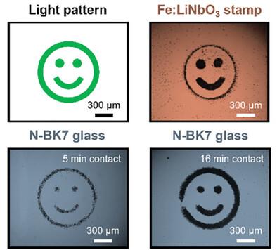
Photovoltaic Fe:LiNbO3 is an outstanding material platform able to photo-generate versatile charge patterns, useful for a broad variety of applications. However, in some cases, its photorefractive effect, light absorption, and active ferroelectric properties may interfere with the optimum operation of certain devices based on Fe:LiNbO3. Here, a novel optoelectronic method is proposed and demonstrated to transfer photovoltaic charge patterns from Fe:LiNbO3 to non-photovoltaic passive substrates, thus removing these possible limitations. The method, denominated as photovoltaic charge lithography (PVCL), resembles the operation of a stamp and does not require external high-voltage supplies or electron/ion beams. Upon contact between the active Fe:LiNbO3 stamp and a passive dielectric substrate, the light-induced charge pattern can be faithfully mirrored on the passive substrate. The imprinted pattern is probed and characterized by dielectrophoretic and electrophoretic particle trapping. The results reveal that the charge builds up on the passive substrate during contact, allowing charge tunability. Moreover, arbitrary charge distributions can be flexibly tailored, using scanning laser beams or spatially structured light. Overall, PVCL opens the possibility of printing complex 1D/2D charge patterns of controlled polarity on different passive dielectric materials, enhancing the technological potential of Fe:LiNbO3 photovoltaic platforms.

使用 Fe:LiNbO3 印模在无源介质基底上进行光伏电荷光刻技术
光伏铁铌酸锂是一种出色的材料平台,能够通过光产生多种电荷模式,应用广泛。然而,在某些情况下,其光折射效应、光吸收和活性铁电特性可能会干扰某些基于 Fe:LiNbO3 的设备的最佳运行。本文提出并演示了一种新颖的光电方法,可将光伏电荷模式从 Fe:LiNbO3 转移到非光伏无源基底上,从而消除这些可能存在的限制。这种方法被称为光伏电荷光刻(PVCL),类似于印章的操作,不需要外部高压电源或电子/离子束。当有源铁铌酸锂印章与无源电介质基底接触时,光诱导电荷图案可以在无源基底上如实反映出来。压印图案可通过介电泳和电泳粒子捕获进行探测和表征。结果表明,电荷在接触过程中会在无源基底上形成,从而实现电荷的可调节性。此外,还可以利用扫描激光束或空间结构光灵活定制任意电荷分布。总之,PVCL 为在不同的无源电介质材料上打印极性可控的复杂一维/二维电荷图案提供了可能性,从而提高了铁铌酸锂光伏平台的技术潜力。
本文章由计算机程序翻译,如有差异,请以英文原文为准。
求助全文
约1分钟内获得全文
求助全文
来源期刊

Advanced Electronic Materials
NANOSCIENCE & NANOTECHNOLOGYMATERIALS SCIE-MATERIALS SCIENCE, MULTIDISCIPLINARY
CiteScore
11.00
自引率
3.20%
发文量
433
期刊介绍:
Advanced Electronic Materials is an interdisciplinary forum for peer-reviewed, high-quality, high-impact research in the fields of materials science, physics, and engineering of electronic and magnetic materials. It includes research on physics and physical properties of electronic and magnetic materials, spintronics, electronics, device physics and engineering, micro- and nano-electromechanical systems, and organic electronics, in addition to fundamental research.
 求助内容:
求助内容: 应助结果提醒方式:


