Heterogeneous wafer bonding of ultra-wide bandgap Ga2O3: A review

IF 10 2区 材料科学 Q1 MATERIALS SCIENCE, MULTIDISCIPLINARY
Xiao Qin , Jieqiong Zhang , Jun Liu , Bo Zhao , Chengguo Li , Qian Wan , Cong Jiang , Jiayun Wei , Wei Han , Baoyuan Wang , Lin Lv , Xu Chen , Houzhao Wan , Hao Wang
{"title":"Heterogeneous wafer bonding of ultra-wide bandgap Ga2O3: A review","authors":"Xiao Qin ,&nbsp;Jieqiong Zhang ,&nbsp;Jun Liu ,&nbsp;Bo Zhao ,&nbsp;Chengguo Li ,&nbsp;Qian Wan ,&nbsp;Cong Jiang ,&nbsp;Jiayun Wei ,&nbsp;Wei Han ,&nbsp;Baoyuan Wang ,&nbsp;Lin Lv ,&nbsp;Xu Chen ,&nbsp;Houzhao Wan ,&nbsp;Hao Wang","doi":"10.1016/j.mtphys.2024.101557","DOIUrl":null,"url":null,"abstract":"<div><div>Gallium oxide (Ga<sub>2</sub>O<sub>3</sub>), with its ultra-wide bandgap (∼4.8 eV) and high theoretical breakdown field (8 MV/cm), holds significant research value and promising application in power electronics and microwave radio-frequency (RF) devices. However, the extremely low thermal conductivity of Ga<sub>2</sub>O<sub>3</sub> severely impedes the fabrication of complicated structures and the optimization of device performance. The wafer bonding technology, as a method to fabricate heterogeneous structures materials, newly applied on Ga<sub>2</sub>O<sub>3</sub> to fabricate Ga<sub>2</sub>O<sub>3</sub> hybrid materials. This paper reviews the wafer bonding technology for ultra-wide bandgap Ga<sub>2</sub>O<sub>3</sub> material based on plasma activation and room-temperature surface activation, as well as the heterogeneous integration with silicon (Si), silicon carbide (SiC), and diamond. The effects of various wafer bonding methods on the bonding quality, thermal, and electrical properties are systematically summarized. Finally, the advancements of Ga<sub>2</sub>O<sub>3</sub>-based heterogeneous structures in the applications of power, RF, and optoelectronic devices are summarized. This review aims to address the key challenges in Ga<sub>2</sub>O<sub>3</sub> material through an understanding of principles and development of bonding technology, thereby facilitating the practical application of Ga<sub>2</sub>O<sub>3</sub>-based devices.</div></div>","PeriodicalId":18253,"journal":{"name":"Materials Today Physics","volume":"48 ","pages":"Article 101557"},"PeriodicalIF":10.0000,"publicationDate":"2024-09-20","publicationTypes":"Journal Article","fieldsOfStudy":null,"isOpenAccess":false,"openAccessPdf":"","citationCount":"0","resultStr":null,"platform":"Semanticscholar","paperid":null,"PeriodicalName":"Materials Today Physics","FirstCategoryId":"88","ListUrlMain":"https://www.sciencedirect.com/science/article/pii/S2542529324002335","RegionNum":2,"RegionCategory":"材料科学","ArticlePicture":[],"TitleCN":null,"AbstractTextCN":null,"PMCID":null,"EPubDate":"","PubModel":"","JCR":"Q1","JCRName":"MATERIALS SCIENCE, MULTIDISCIPLINARY","Score":null,"Total":0}
引用次数: 0

Abstract

Gallium oxide (Ga2O3), with its ultra-wide bandgap (∼4.8 eV) and high theoretical breakdown field (8 MV/cm), holds significant research value and promising application in power electronics and microwave radio-frequency (RF) devices. However, the extremely low thermal conductivity of Ga2O3 severely impedes the fabrication of complicated structures and the optimization of device performance. The wafer bonding technology, as a method to fabricate heterogeneous structures materials, newly applied on Ga2O3 to fabricate Ga2O3 hybrid materials. This paper reviews the wafer bonding technology for ultra-wide bandgap Ga2O3 material based on plasma activation and room-temperature surface activation, as well as the heterogeneous integration with silicon (Si), silicon carbide (SiC), and diamond. The effects of various wafer bonding methods on the bonding quality, thermal, and electrical properties are systematically summarized. Finally, the advancements of Ga2O3-based heterogeneous structures in the applications of power, RF, and optoelectronic devices are summarized. This review aims to address the key challenges in Ga2O3 material through an understanding of principles and development of bonding technology, thereby facilitating the practical application of Ga2O3-based devices.
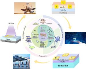
Abstract Image

超宽带隙 Ga2O3 的异质晶片键合:综述
氧化镓(Ga2O3)具有超宽带隙(∼4.8 eV)和高理论击穿场(8 MV/cm),在电力电子和微波射频(RF)器件领域具有重要的研究价值和应用前景。然而,Ga2O3 极低的热导率严重阻碍了复杂结构的制造和器件性能的优化。晶圆键合技术作为一种制造异质结构材料的方法,新近被应用到 Ga2O3 上,以制造 Ga2O3 混合材料。本文综述了基于等离子体活化和室温表面活化的超宽带隙 Ga2O3 材料晶圆键合技术,以及与硅(Si)、碳化硅(SiC)和金刚石的异质集成。系统地总结了各种晶片键合方法对键合质量、热性能和电性能的影响。最后,总结了基于 Ga2O3 的异质结构在功率、射频和光电器件应用方面的进展。本综述旨在通过对原理的理解和键合技术的发展来解决 Ga2O3 材料所面临的关键挑战,从而促进基于 Ga2O3 的器件的实际应用。
本文章由计算机程序翻译,如有差异,请以英文原文为准。
求助全文
约1分钟内获得全文 求助全文
来源期刊
Materials Today Physics
Materials Today Physics Materials Science-General Materials Science
CiteScore
14.00
自引率
7.80%
发文量
284
审稿时长
15 days
期刊介绍: Materials Today Physics is a multi-disciplinary journal focused on the physics of materials, encompassing both the physical properties and materials synthesis. Operating at the interface of physics and materials science, this journal covers one of the largest and most dynamic fields within physical science. The forefront research in materials physics is driving advancements in new materials, uncovering new physics, and fostering novel applications at an unprecedented pace.
×
引用
GB/T 7714-2015
复制
MLA
复制
APA
复制
导出至
BibTeX EndNote RefMan NoteFirst NoteExpress
×
提示
您的信息不完整,为了账户安全,请先补充。
现在去补充
×
提示
您因"违规操作"
具体请查看互助需知
我知道了
×
提示
确定
请完成安全验证×
copy
已复制链接
快去分享给好友吧!
我知道了
右上角分享
点击右上角分享
0
联系我们:info@booksci.cn Book学术提供免费学术资源搜索服务,方便国内外学者检索中英文文献。致力于提供最便捷和优质的服务体验。 Copyright © 2023 布克学术 All rights reserved.
京ICP备2023020795号-1
ghs 京公网安备 11010802042870号
Book学术文献互助
Book学术文献互助群
群 号:481959085
Book学术官方微信