Zhi-Hong Zhang, Xiao-Bing Hou, Shang-Heng Li, Zhi-Peng Wei, Jin-Chao Wei, Peng Li and Shuang-Peng Wang
{"title":"Van der Waals integration of phase-pure 2D perovskite sheets and GaAs nanowires for self-driven photodetector†","authors":"Zhi-Hong Zhang, Xiao-Bing Hou, Shang-Heng Li, Zhi-Peng Wei, Jin-Chao Wei, Peng Li and Shuang-Peng Wang","doi":"10.1039/D4TC02994A","DOIUrl":null,"url":null,"abstract":"<p >Semiconductor heterostructures hold significant importance for exploring novel functional optoelectronic devices, but the chemical instability and soft lattice framework of perovskites significantly hinder the efficient heterogeneous integration with other perovskite or semiconductor materials. Herein, based on the large-area phase-pure 2D perovskite sheets, a BA<small><sub>2</sub></small>MA<small><sub>2</sub></small>Pb<small><sub>3</sub></small>I<small><sub>10</sub></small>/GaAs van der Waals (vdW) heterostructure has been successfully constructed. The favorable vdW contacts allow the device to be cut-off at forward bias with a remarkably low dark current of 1.94 pA. This endows the heterostructure device with excellent detection performance, achieving a linear dynamic range of 80.9 dB and a detectivity of 6.17 × 10<small><sup>10</sup></small> Jones. Additionally, the interfacial potential of the heterostructure enables the device to operate in a self-driven manner across broad spectral ranges from ultraviolet to near-infrared. Our study demonstrates efficient vdW integration based on perovskite and provides a new foundation for constructing perovskite vdW heterostructures.</p>","PeriodicalId":84,"journal":{"name":"Journal of Materials Chemistry C","volume":null,"pages":null},"PeriodicalIF":5.7000,"publicationDate":"2024-08-28","publicationTypes":"Journal Article","fieldsOfStudy":null,"isOpenAccess":false,"openAccessPdf":"https://pubs.rsc.org/en/content/articlepdf/2024/tc/d4tc02994a?page=search","citationCount":"0","resultStr":null,"platform":"Semanticscholar","paperid":null,"PeriodicalName":"Journal of Materials Chemistry C","FirstCategoryId":"1","ListUrlMain":"https://pubs.rsc.org/en/content/articlelanding/2024/tc/d4tc02994a","RegionNum":2,"RegionCategory":"材料科学","ArticlePicture":[],"TitleCN":null,"AbstractTextCN":null,"PMCID":null,"EPubDate":"","PubModel":"","JCR":"Q2","JCRName":"MATERIALS SCIENCE, MULTIDISCIPLINARY","Score":null,"Total":0}
引用次数: 0
Abstract
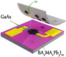
Semiconductor heterostructures hold significant importance for exploring novel functional optoelectronic devices, but the chemical instability and soft lattice framework of perovskites significantly hinder the efficient heterogeneous integration with other perovskite or semiconductor materials. Herein, based on the large-area phase-pure 2D perovskite sheets, a BA2MA2Pb3I10/GaAs van der Waals (vdW) heterostructure has been successfully constructed. The favorable vdW contacts allow the device to be cut-off at forward bias with a remarkably low dark current of 1.94 pA. This endows the heterostructure device with excellent detection performance, achieving a linear dynamic range of 80.9 dB and a detectivity of 6.17 × 10¹⁰ Jones. Additionally, the interfacial potential of the heterostructure enables the device to operate in a self-driven manner across broad spectral ranges from ultraviolet to near-infrared. Our study demonstrates efficient vdW integration based on perovskite and provides a new foundation for constructing perovskite vdW heterostructures.
期刊介绍:
The Journal of Materials Chemistry is divided into three distinct sections, A, B, and C, each catering to specific applications of the materials under study:
Journal of Materials Chemistry A focuses primarily on materials intended for applications in energy and sustainability.
Journal of Materials Chemistry B specializes in materials designed for applications in biology and medicine.
Journal of Materials Chemistry C is dedicated to materials suitable for applications in optical, magnetic, and electronic devices.
Example topic areas within the scope of Journal of Materials Chemistry C are listed below. This list is neither exhaustive nor exclusive.
Bioelectronics
Conductors
Detectors
Dielectrics
Displays
Ferroelectrics
Lasers
LEDs
Lighting
Liquid crystals
Memory
Metamaterials
Multiferroics
Photonics
Photovoltaics
Semiconductors
Sensors
Single molecule conductors
Spintronics
Superconductors
Thermoelectrics
Topological insulators
Transistors


 求助内容:
求助内容: 应助结果提醒方式:


