Tuning the Resistance of a VO2 Junction by Focused Laser Beam and Atomic Force Microscopy

IF 5.3 2区 材料科学 Q2 MATERIALS SCIENCE, MULTIDISCIPLINARY
Zhuoqun Fang, Melissa Alzate-Banguero, Amit R. Rajapurohita, Forrest Simmons, Erica W. Carlson, Zhuoying Chen, Lionel Aigouy, Alexandre Zimmers
{"title":"Tuning the Resistance of a VO2 Junction by Focused Laser Beam and Atomic Force Microscopy","authors":"Zhuoqun Fang, Melissa Alzate-Banguero, Amit R. Rajapurohita, Forrest Simmons, Erica W. Carlson, Zhuoying Chen, Lionel Aigouy, Alexandre Zimmers","doi":"10.1002/aelm.202400249","DOIUrl":null,"url":null,"abstract":"Vanadium Dioxide (VO<sub>2</sub>) is a material that exhibits a phase transition from an insulating state to a metallic state at ≈68 °C. During a temperature cycle consisting of warming followed by cooling, the resistivity of VO<sub>2</sub> changes by several orders of magnitude over the course of the hysteresis loop. Using a focused laser beam (λ = 532 nm), it is shown that it is possible to optically generate micron-sized metallic patterns within the insulating phase of a VO<sub>2</sub> planar junction which can be used to tune, on demand, the resistance of the VO<sub>2</sub> junction. A resistor network simulation is used to characterize the resulting resistance drops in the devices. These patterns persist while the base temperature is held constant within the hysteretic region while being easily removed totally by simply lowering the base temperature. Surprisingly, it is also observed that the pattern can be partially erased using an atomic force microscope (AFM) tip on the submicron scale. This erasing process can be qualitatively explained by the temperature difference between the VO<sub>2</sub> surface and the tip which acts as a local cooler. This optical and AFM resistive fine-tuning offers the possibility of creating controllable synaptic weights between room-temperature VO<sub>2</sub> neuristors.","PeriodicalId":110,"journal":{"name":"Advanced Electronic Materials","volume":"49 1","pages":""},"PeriodicalIF":5.3000,"publicationDate":"2024-09-11","publicationTypes":"Journal Article","fieldsOfStudy":null,"isOpenAccess":false,"openAccessPdf":"","citationCount":"0","resultStr":null,"platform":"Semanticscholar","paperid":null,"PeriodicalName":"Advanced Electronic Materials","FirstCategoryId":"88","ListUrlMain":"https://doi.org/10.1002/aelm.202400249","RegionNum":2,"RegionCategory":"材料科学","ArticlePicture":[],"TitleCN":null,"AbstractTextCN":null,"PMCID":null,"EPubDate":"","PubModel":"","JCR":"Q2","JCRName":"MATERIALS SCIENCE, MULTIDISCIPLINARY","Score":null,"Total":0}
引用次数: 0

Abstract

Vanadium Dioxide (VO2) is a material that exhibits a phase transition from an insulating state to a metallic state at ≈68 °C. During a temperature cycle consisting of warming followed by cooling, the resistivity of VO2 changes by several orders of magnitude over the course of the hysteresis loop. Using a focused laser beam (λ = 532 nm), it is shown that it is possible to optically generate micron-sized metallic patterns within the insulating phase of a VO2 planar junction which can be used to tune, on demand, the resistance of the VO2 junction. A resistor network simulation is used to characterize the resulting resistance drops in the devices. These patterns persist while the base temperature is held constant within the hysteretic region while being easily removed totally by simply lowering the base temperature. Surprisingly, it is also observed that the pattern can be partially erased using an atomic force microscope (AFM) tip on the submicron scale. This erasing process can be qualitatively explained by the temperature difference between the VO2 surface and the tip which acts as a local cooler. This optical and AFM resistive fine-tuning offers the possibility of creating controllable synaptic weights between room-temperature VO2 neuristors.
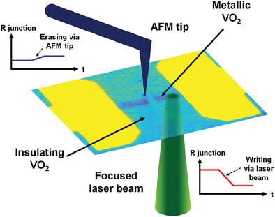
Abstract Image

通过聚焦激光束和原子力显微镜调节 VO2 结的电阻
二氧化钒(VO2)是一种在 ≈68 ℃ 时从绝缘状态向金属状态发生相变的材料。在先升温后降温的温度循环过程中,二氧化钒的电阻率在滞后循环过程中会发生几个数量级的变化。研究表明,利用聚焦激光束(λ = 532 nm),可以在 VO2 平面结的绝缘相内光学生成微米级的金属图案,从而根据需要调节 VO2 结的电阻。电阻网络模拟用于描述器件中产生的电阻下降。当基底温度在滞后区域内保持不变时,这些模式会持续存在,而只要降低基底温度,就能轻易地完全消除这些模式。令人惊奇的是,我们还观察到,使用原子力显微镜(AFM)尖端可以部分擦除亚微米尺度的图案。这种擦除过程可以用 VO2 表面和针尖之间的温差来定性解释,因为针尖起到了局部冷却的作用。这种光学和原子力显微镜电阻微调为在室温 VO2 神经元之间建立可控的突触权重提供了可能。
本文章由计算机程序翻译,如有差异,请以英文原文为准。
求助全文
约1分钟内获得全文 求助全文
来源期刊
Advanced Electronic Materials
Advanced Electronic Materials NANOSCIENCE & NANOTECHNOLOGYMATERIALS SCIE-MATERIALS SCIENCE, MULTIDISCIPLINARY
CiteScore
11.00
自引率
3.20%
发文量
433
期刊介绍: Advanced Electronic Materials is an interdisciplinary forum for peer-reviewed, high-quality, high-impact research in the fields of materials science, physics, and engineering of electronic and magnetic materials. It includes research on physics and physical properties of electronic and magnetic materials, spintronics, electronics, device physics and engineering, micro- and nano-electromechanical systems, and organic electronics, in addition to fundamental research.
×
引用
GB/T 7714-2015
复制
MLA
复制
APA
复制
导出至
BibTeX EndNote RefMan NoteFirst NoteExpress
×
提示
您的信息不完整,为了账户安全,请先补充。
现在去补充
×
提示
您因"违规操作"
具体请查看互助需知
我知道了
×
提示
确定
请完成安全验证×
copy
已复制链接
快去分享给好友吧!
我知道了
右上角分享
点击右上角分享
0
联系我们:info@booksci.cn Book学术提供免费学术资源搜索服务,方便国内外学者检索中英文文献。致力于提供最便捷和优质的服务体验。 Copyright © 2023 布克学术 All rights reserved.
京ICP备2023020795号-1
ghs 京公网安备 11010802042870号
Book学术文献互助
Book学术文献互助群
群 号:481959085
Book学术官方微信