Sabah. E. Algarni, Atef F. Qasrawi, Najla. M. Khusayfan
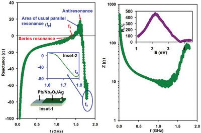
{"title":"High Broadband Optical Absorption and Bandstop Filter Characteristics of Pb/Nb2O5 Interfaces","authors":"Sabah. E. Algarni, Atef F. Qasrawi, Najla. M. Khusayfan","doi":"10.1002/crat.202400136","DOIUrl":null,"url":null,"abstract":"<p>In this study, semitransparent lead films serve as substrates for depositing niobium pentoxide thin films, forming versatile electro-optical devices. Using vacuum evaporation and ion sputtering techniques at ≈10<sup>−5</sup> mbar, stacked layers of crystalline Pb and amorphous Nb<sub>2</sub>O<sub>5</sub> are created. This process reduces free carrier absorption in Nb<sub>2</sub>O<sub>5</sub> and forms Urbach tail states with a width of 0.91 eV. Pb/Nb<sub>2</sub>O<sub>5</sub> thin films exhibit remarkable broadband absorption, exceeding 440% in the visible and 98% in the infrared. Moreover, Pb substrates induce a redshift in Nb<sub>2</sub>O<sub>5</sub>’s energy bandgap. Electrical analysis using impedance spectroscopy on Pb/Nb<sub>2</sub>O<sub>5</sub>/Ag structures reveals their series/parallel resonance and bandstop filter properties. Notably, the bandstop filters exhibit reflection coefficient minima at a notch frequency of 1.66 GHz, with a bandwidth of 280 MHz, return loss of 26 dB, and voltage standing wave ratio of 1.13. These findings underscore the device's potential for wide-ranging electro-optical applications across the electromagnetic spectrum.</p>","PeriodicalId":48935,"journal":{"name":"Crystal Research and Technology","volume":"59 9","pages":""},"PeriodicalIF":1.5000,"publicationDate":"2024-08-06","publicationTypes":"Journal Article","fieldsOfStudy":null,"isOpenAccess":false,"openAccessPdf":"","citationCount":"0","resultStr":null,"platform":"Semanticscholar","paperid":null,"PeriodicalName":"Crystal Research and Technology","FirstCategoryId":"88","ListUrlMain":"https://onlinelibrary.wiley.com/doi/10.1002/crat.202400136","RegionNum":4,"RegionCategory":"材料科学","ArticlePicture":[],"TitleCN":null,"AbstractTextCN":null,"PMCID":null,"EPubDate":"","PubModel":"","JCR":"Q3","JCRName":"Chemistry","Score":null,"Total":0}
引用次数: 0
Abstract
In this study, semitransparent lead films serve as substrates for depositing niobium pentoxide thin films, forming versatile electro-optical devices. Using vacuum evaporation and ion sputtering techniques at ≈10−5 mbar, stacked layers of crystalline Pb and amorphous Nb2O5 are created. This process reduces free carrier absorption in Nb2O5 and forms Urbach tail states with a width of 0.91 eV. Pb/Nb2O5 thin films exhibit remarkable broadband absorption, exceeding 440% in the visible and 98% in the infrared. Moreover, Pb substrates induce a redshift in Nb2O5’s energy bandgap. Electrical analysis using impedance spectroscopy on Pb/Nb2O5/Ag structures reveals their series/parallel resonance and bandstop filter properties. Notably, the bandstop filters exhibit reflection coefficient minima at a notch frequency of 1.66 GHz, with a bandwidth of 280 MHz, return loss of 26 dB, and voltage standing wave ratio of 1.13. These findings underscore the device's potential for wide-ranging electro-optical applications across the electromagnetic spectrum.
期刊介绍:
The journal Crystal Research and Technology is a pure online Journal (since 2012).
Crystal Research and Technology is an international journal examining all aspects of research within experimental, industrial, and theoretical crystallography. The journal covers the relevant aspects of
-crystal growth techniques and phenomena (including bulk growth, thin films)
-modern crystalline materials (e.g. smart materials, nanocrystals, quasicrystals, liquid crystals)
-industrial crystallisation
-application of crystals in materials science, electronics, data storage, and optics
-experimental, simulation and theoretical studies of the structural properties of crystals
-crystallographic computing
 求助内容:
求助内容: 应助结果提醒方式:


