Analysis of Carrier Scattering Mechanisms in AlN/GaN HEMT Heterostructures with an Ultrathin AlN Barrier
Q4 Engineering
引用次数: 0
Abstract
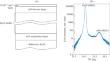
Using the method of molecular beam epitaxy with the plasma activation of nitrogen, experimental AlN/GaN heterostructures (HSs) with an ultrathin AlN barrier are obtained. The layer resistance of the optimized structures is less than 230 Ω/□. The scattering processes that limit the mobility of a two-dimensional electron gas (2DEG) in undoped AlN/GaN HSs with an ultrathin AlN barrier are studied. It is shown that in the range of ns characteristic for AlN/GaN HEMT HSs (ns > 1 × 1013 cm–2), a noticeable contribution to the scattering of charge carriers is made by the roughness of the heterointerface.
带有超薄氮化铝势垒的氮化铝/氮化镓 HEMT 异质结构中的载流子散射机制分析
摘要 利用分子束外延和氮等离子活化的方法,获得了具有超薄氮化铝阻挡层的氮化铝/氮化镓异质结构(HS)。优化结构的层电阻小于 230 Ω/□。研究了限制具有超薄氮化铝势垒的未掺杂氮化铝/氮化镓 HS 中二维电子气体(2DEG)迁移率的散射过程。研究表明,在 AlN/GaN HEMT HS 的 ns 特性范围内(ns > 1 × 1013 cm-2),异质表面的粗糙度对电荷载流子的散射有明显的贡献。
本文章由计算机程序翻译,如有差异,请以英文原文为准。
求助全文
约1分钟内获得全文
求助全文
来源期刊
Russian Microelectronics
Materials Science-Materials Chemistry
CiteScore
0.70
自引率
0.00%
发文量
43
期刊介绍:
Russian Microelectronics covers physical, technological, and some VLSI and ULSI circuit-technical aspects of microelectronics and nanoelectronics; it informs the reader of new trends in submicron optical, x-ray, electron, and ion-beam lithography technology; dry processing techniques, etching, doping; and deposition and planarization technology. Significant space is devoted to problems arising in the application of proton, electron, and ion beams, plasma, etc. Consideration is given to new equipment, including cluster tools and control in situ and submicron CMOS, bipolar, and BICMOS technologies. The journal publishes papers addressing problems of molecular beam epitaxy and related processes; heterojunction devices and integrated circuits; the technology and devices of nanoelectronics; and the fabrication of nanometer scale devices, including new device structures, quantum-effect devices, and superconducting devices. The reader will find papers containing news of the diagnostics of surfaces and microelectronic structures, the modeling of technological processes and devices in micro- and nanoelectronics, including nanotransistors, and solid state qubits.
 求助内容:
求助内容: 应助结果提醒方式:


