A. A. Lomov, B. M. Seredin, S. Yu. Martyushov, A. A. Tatarintsev, V. P. Popov, A. V. Malibashev
{"title":"Structural Features and Electrical Properties of Si(Al) Thermomigration Channels for High-Voltage Photoelectric Converters","authors":"A. A. Lomov, B. M. Seredin, S. Yu. Martyushov, A. A. Tatarintsev, V. P. Popov, A. V. Malibashev","doi":"10.1134/s1063739724600109","DOIUrl":null,"url":null,"abstract":"<h3 data-test=\"abstract-sub-heading\">Abstract</h3><p>The results of a study of the structural features and electrical properties of the end-to-end thermomigration (ThM) of the <i>p</i>-channels of Si(Al) in a silicon wafer are presented. Structural studies are carried out using X-ray methods of projection topography, diffraction reflection curves, and scanning electron microscopy (SEM). It is shown that the channel-matrix interface is coherent without the formation of misfit dislocations. The possibility is shown of using an array of the ThM of the <i>p</i>-channels of 15 elements for the formation of a monolithic photoelectric solar module in a Si(111)-based silicon wafer of <i>p</i>-channels 100 µm wide with walls in the plane <span>\\(\\left( {1\\bar {1}0} \\right)\\)</span>. The monolithic solar module has a conversion efficiency of 13.1%, an open circuit voltage of 8.5 V, and a short circuit current density of 33 mA/cm<sup>2</sup>.</p>","PeriodicalId":21534,"journal":{"name":"Russian Microelectronics","volume":"36 1","pages":""},"PeriodicalIF":0.0000,"publicationDate":"2024-06-04","publicationTypes":"Journal Article","fieldsOfStudy":null,"isOpenAccess":false,"openAccessPdf":"","citationCount":"0","resultStr":null,"platform":"Semanticscholar","paperid":null,"PeriodicalName":"Russian Microelectronics","FirstCategoryId":"1085","ListUrlMain":"https://doi.org/10.1134/s1063739724600109","RegionNum":0,"RegionCategory":null,"ArticlePicture":[],"TitleCN":null,"AbstractTextCN":null,"PMCID":null,"EPubDate":"","PubModel":"","JCR":"Q4","JCRName":"Engineering","Score":null,"Total":0}
引用次数: 0
Abstract
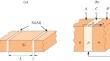
The results of a study of the structural features and electrical properties of the end-to-end thermomigration (ThM) of the p-channels of Si(Al) in a silicon wafer are presented. Structural studies are carried out using X-ray methods of projection topography, diffraction reflection curves, and scanning electron microscopy (SEM). It is shown that the channel-matrix interface is coherent without the formation of misfit dislocations. The possibility is shown of using an array of the ThM of the p-channels of 15 elements for the formation of a monolithic photoelectric solar module in a Si(111)-based silicon wafer of p-channels 100 µm wide with walls in the plane \(\left( {1\bar {1}0} \right)\). The monolithic solar module has a conversion efficiency of 13.1%, an open circuit voltage of 8.5 V, and a short circuit current density of 33 mA/cm2.
期刊介绍:
Russian Microelectronics covers physical, technological, and some VLSI and ULSI circuit-technical aspects of microelectronics and nanoelectronics; it informs the reader of new trends in submicron optical, x-ray, electron, and ion-beam lithography technology; dry processing techniques, etching, doping; and deposition and planarization technology. Significant space is devoted to problems arising in the application of proton, electron, and ion beams, plasma, etc. Consideration is given to new equipment, including cluster tools and control in situ and submicron CMOS, bipolar, and BICMOS technologies. The journal publishes papers addressing problems of molecular beam epitaxy and related processes; heterojunction devices and integrated circuits; the technology and devices of nanoelectronics; and the fabrication of nanometer scale devices, including new device structures, quantum-effect devices, and superconducting devices. The reader will find papers containing news of the diagnostics of surfaces and microelectronic structures, the modeling of technological processes and devices in micro- and nanoelectronics, including nanotransistors, and solid state qubits.
 求助内容:
求助内容: 应助结果提醒方式:


