Zuzanna Molenda, Sylvain Chambon, Dario M. Bassani, Lionel Hirsch
{"title":"Electronic Doping in Perovskite Solar Cells","authors":"Zuzanna Molenda, Sylvain Chambon, Dario M. Bassani, Lionel Hirsch","doi":"10.1002/aelm.202400090","DOIUrl":null,"url":null,"abstract":"<p>The popularity of metal halide perovskites is in part the result of their versatility in numerous applications. To date, perovskites are used in their intrinsic, undoped form, as the doping of these materials is not yet adequately mastered. Herein, the recently reported electronic doping of CH<sub>3</sub>NH<sub>3</sub>PbI<sub>3</sub> is employed to fabricate perovskite solar cells in which the interfacial electron transport layer (ETL) is replaced by n-doping of one side of the perovskite film. The doping involves the incorporation of metastable Sm<sup>2+</sup> ions that undergo an in situ oxidation to Sm<sup>3+</sup>, releasing electrons to the conduction band to render the perovskite n-type. In spite of the lack of an ETL, these solar cells have the same efficiency as the samples with the ETL. The open circuit voltage of the doped solar cells increases proportionally to the doping concentration due to the narrowing of the depletion layer thickness at the interface of the perovskite and the top electrode, reaching the value of ≈1 V for the doped ETL-free device, the same as for the reference sample. These proof-of-concept results represent the first step toward perovskite-based devices incorporating a p-n homojunction.</p>","PeriodicalId":110,"journal":{"name":"Advanced Electronic Materials","volume":"10 10","pages":""},"PeriodicalIF":5.3000,"publicationDate":"2024-05-26","publicationTypes":"Journal Article","fieldsOfStudy":null,"isOpenAccess":false,"openAccessPdf":"https://onlinelibrary.wiley.com/doi/epdf/10.1002/aelm.202400090","citationCount":"0","resultStr":null,"platform":"Semanticscholar","paperid":null,"PeriodicalName":"Advanced Electronic Materials","FirstCategoryId":"88","ListUrlMain":"https://onlinelibrary.wiley.com/doi/10.1002/aelm.202400090","RegionNum":2,"RegionCategory":"材料科学","ArticlePicture":[],"TitleCN":null,"AbstractTextCN":null,"PMCID":null,"EPubDate":"","PubModel":"","JCR":"Q2","JCRName":"MATERIALS SCIENCE, MULTIDISCIPLINARY","Score":null,"Total":0}
引用次数: 0
Abstract
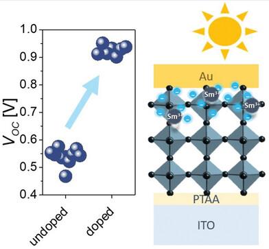
The popularity of metal halide perovskites is in part the result of their versatility in numerous applications. To date, perovskites are used in their intrinsic, undoped form, as the doping of these materials is not yet adequately mastered. Herein, the recently reported electronic doping of CH3NH3PbI3 is employed to fabricate perovskite solar cells in which the interfacial electron transport layer (ETL) is replaced by n-doping of one side of the perovskite film. The doping involves the incorporation of metastable Sm2+ ions that undergo an in situ oxidation to Sm3+, releasing electrons to the conduction band to render the perovskite n-type. In spite of the lack of an ETL, these solar cells have the same efficiency as the samples with the ETL. The open circuit voltage of the doped solar cells increases proportionally to the doping concentration due to the narrowing of the depletion layer thickness at the interface of the perovskite and the top electrode, reaching the value of ≈1 V for the doped ETL-free device, the same as for the reference sample. These proof-of-concept results represent the first step toward perovskite-based devices incorporating a p-n homojunction.
期刊介绍:
Advanced Electronic Materials is an interdisciplinary forum for peer-reviewed, high-quality, high-impact research in the fields of materials science, physics, and engineering of electronic and magnetic materials. It includes research on physics and physical properties of electronic and magnetic materials, spintronics, electronics, device physics and engineering, micro- and nano-electromechanical systems, and organic electronics, in addition to fundamental research.

 求助内容:
求助内容: 应助结果提醒方式:


