Achieving Near-Ideal Subthreshold Swing in P-Type WSe2 Field-Effect Transistors
IF 5.3
2区 材料科学
Q2 MATERIALS SCIENCE, MULTIDISCIPLINARY
引用次数: 0
Abstract
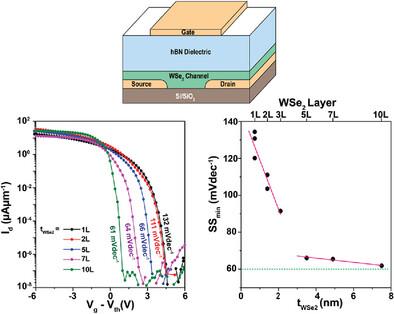
The pursuit of near-ideal subthreshold swing (SS) ≈ 60 mV dec−1 is a primary driving force to realize the power-efficient field-effect transistors (FETs). This challenge is particularly pronounced in 2D material-based FETs, where the presence of a large interface trap density (Dit) imposes limitations on electrostatic control, consequently escalating power consumption. In this study, the gate controllability of 2D FETs is systematically analyzed by fabricating pre-patterned van der Waals (vdW)-contacted p-FETs, varying the WSe2 channel thickness from monolayer to ten-layer. As a result, the channel thickness is optimized to achieve efficient gate controllability while minimizing Dit. The findings demonstrate negligible hysteresis and excellent subthreshold swing (SSmin) close to the thermal limit (≈60 mV dec−1), with a corresponding Dit of ≈1010 cm−2 eV−1, comparable to Dit values observed in state-of-the-art Si transistors, when utilizing WSe2 channel thicknesses ≥ five-layer. However, reducing the WSe2 channel thickness below the trilayer, SSmin (≈91 mV dec−1) deviates from the thermal limit, attributed to a comparatively higher Dit (≈1011 cm−2 eV−1), despite the still lower than values reported for surface-contacted 2D transistors. Furthermore, all devices exhibit consistent p-type characteristics, featuring a high ION/IOFF ratio, high mobility, and excellent electrical stability confirmed over several months.
在 P 型 WSe2 场效应晶体管中实现接近理想的次阈值波动
追求接近理想的阈下摆幅(SS)≈ 60 mV dec-1是实现高能效场效应晶体管(FET)的主要动力。这一挑战在基于二维材料的场效应晶体管中尤为突出,因为大量界面陷阱密度(Dit)的存在限制了静电控制,从而导致功耗上升。在本研究中,通过制造预图案化的范德华(vdW)接触 p 型场效应晶体管,改变 WSe2 沟道厚度(从单层到十层),系统分析了二维场效应晶体管的栅极可控性。因此,沟道厚度得到了优化,从而实现了高效的栅极可控性,同时将 Dit 降到了最低。研究结果表明,当使用的 WSe2 沟道厚度≥ 5 层时,可忽略的滞后和接近热极限(≈60 mV dec-1)的出色阈下摆幅(SSmin),以及相应的 Dit ≈1010 cm-2 eV-1,与最先进的硅晶体管中观察到的 Dit 值相当。然而,当 WSe2 沟道厚度减小到三层以下时,SSmin(≈91 mV dec-1)偏离了热极限,这归因于相对较高的 Dit(≈1011 cm-2 eV-1),尽管仍低于表面接触式二维晶体管的报告值。此外,所有器件都表现出一致的 p 型特性,具有高 ION/IOFF 比、高迁移率和卓越的电稳定性,并经过数月验证。
本文章由计算机程序翻译,如有差异,请以英文原文为准。
求助全文
约1分钟内获得全文
求助全文
来源期刊
Advanced Electronic Materials
NANOSCIENCE & NANOTECHNOLOGYMATERIALS SCIE-MATERIALS SCIENCE, MULTIDISCIPLINARY
CiteScore
11.00
自引率
3.20%
发文量
433
期刊介绍:
Advanced Electronic Materials is an interdisciplinary forum for peer-reviewed, high-quality, high-impact research in the fields of materials science, physics, and engineering of electronic and magnetic materials. It includes research on physics and physical properties of electronic and magnetic materials, spintronics, electronics, device physics and engineering, micro- and nano-electromechanical systems, and organic electronics, in addition to fundamental research.
文献相关原料
| 公司名称 | 产品信息 | 采购帮参考价格 |
|---|
 求助内容:
求助内容: 应助结果提醒方式:


