K. A. Tsarik, N. P. Nekrasov, V. K. Nevolin, I. I. Bobrinetskiy
{"title":"Features of the Formation of Suspended Graphene Structures over an Array of Microsized Pores","authors":"K. A. Tsarik, N. P. Nekrasov, V. K. Nevolin, I. I. Bobrinetskiy","doi":"10.1134/s1063739723070193","DOIUrl":null,"url":null,"abstract":"<h3 data-test=\"abstract-sub-heading\">Abstract</h3><p>Structures based on suspended graphene are promising elements for problems in photonics and sensory electronics due to the possibility of the elimination of trap states in the substrate and the increase in the speed and sensitivity of the graphene layer. The development of techniques for introducing carbon nanostructures in silicon technology to create micro- and nanoelectronic devices is also relevant. In this paper, the features of the technique for the formation of a silicon membrane and pores in it, as well as the deposition of graphene on silicon membranes, are presented. The Raman spectra of suspended graphene showing a shift of the G-peak by 4.5 cm<sup>–1</sup> and the 2D peak by 7.5 cm<sup>–1</sup> relative to the peaks of the graphene lying on silicon are obtained. Using the curves of the approach and retraction of the probe of an atomic force microscope, the possible deflection of the suspended graphene is studied, showing the distances at which the attractive and repulsive forces are located in the probe–suspended graphene system. It is established that the significant deflection of graphene, by 1 µm at a pore diameter of 5 µm, makes laser focusing is difficult. This primarily affects the use of such structures as a base for a gas or fluid sensor of various organic compounds, as well as for suspended graphene-based transistors.</p>","PeriodicalId":21534,"journal":{"name":"Russian Microelectronics","volume":"18 1","pages":""},"PeriodicalIF":0.0000,"publicationDate":"2024-02-15","publicationTypes":"Journal Article","fieldsOfStudy":null,"isOpenAccess":false,"openAccessPdf":"","citationCount":"0","resultStr":null,"platform":"Semanticscholar","paperid":null,"PeriodicalName":"Russian Microelectronics","FirstCategoryId":"1085","ListUrlMain":"https://doi.org/10.1134/s1063739723070193","RegionNum":0,"RegionCategory":null,"ArticlePicture":[],"TitleCN":null,"AbstractTextCN":null,"PMCID":null,"EPubDate":"","PubModel":"","JCR":"Q4","JCRName":"Engineering","Score":null,"Total":0}
引用次数: 0
Abstract
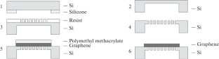
Structures based on suspended graphene are promising elements for problems in photonics and sensory electronics due to the possibility of the elimination of trap states in the substrate and the increase in the speed and sensitivity of the graphene layer. The development of techniques for introducing carbon nanostructures in silicon technology to create micro- and nanoelectronic devices is also relevant. In this paper, the features of the technique for the formation of a silicon membrane and pores in it, as well as the deposition of graphene on silicon membranes, are presented. The Raman spectra of suspended graphene showing a shift of the G-peak by 4.5 cm–1 and the 2D peak by 7.5 cm–1 relative to the peaks of the graphene lying on silicon are obtained. Using the curves of the approach and retraction of the probe of an atomic force microscope, the possible deflection of the suspended graphene is studied, showing the distances at which the attractive and repulsive forces are located in the probe–suspended graphene system. It is established that the significant deflection of graphene, by 1 µm at a pore diameter of 5 µm, makes laser focusing is difficult. This primarily affects the use of such structures as a base for a gas or fluid sensor of various organic compounds, as well as for suspended graphene-based transistors.
期刊介绍:
Russian Microelectronics covers physical, technological, and some VLSI and ULSI circuit-technical aspects of microelectronics and nanoelectronics; it informs the reader of new trends in submicron optical, x-ray, electron, and ion-beam lithography technology; dry processing techniques, etching, doping; and deposition and planarization technology. Significant space is devoted to problems arising in the application of proton, electron, and ion beams, plasma, etc. Consideration is given to new equipment, including cluster tools and control in situ and submicron CMOS, bipolar, and BICMOS technologies. The journal publishes papers addressing problems of molecular beam epitaxy and related processes; heterojunction devices and integrated circuits; the technology and devices of nanoelectronics; and the fabrication of nanometer scale devices, including new device structures, quantum-effect devices, and superconducting devices. The reader will find papers containing news of the diagnostics of surfaces and microelectronic structures, the modeling of technological processes and devices in micro- and nanoelectronics, including nanotransistors, and solid state qubits.
 求助内容:
求助内容: 应助结果提醒方式:


