A. V. Miakonkikh, V. O. Kuzmenko, A. E. Melnikov, K. V. Rudenko
{"title":"Tapered Silicon Oxide Etching for Creation of Capacitor Structures for Measurement of Dielectric Characteristics","authors":"A. V. Miakonkikh, V. O. Kuzmenko, A. E. Melnikov, K. V. Rudenko","doi":"10.1134/s1063739723700695","DOIUrl":null,"url":null,"abstract":"<h3 data-test=\"abstract-sub-heading\">Abstract</h3><p>The article develops the possibility of forming silicon oxide structures with tapered walls using dry etching methods, including a two-stage process involving the formation of a tapered photoresist mask and plasma etching of the silicon oxide. A study of the process of tapered resist etching was carried out. The influence of plasma parameters and composition on the etching process was studied, plasma diagnostics were carried out using Langmuir probe and optical emission actinometry methods, and the mechanisms of tapered resist etching were suggested. The etching process was optimized and structures with a resist thickness of 400 nm and a sidewall angle of up to 61° were obtained. A subsequent SiO<sub>2</sub> etching process allowed the slope of the resist to be transferred. The slope of the SiO<sub>2</sub> wall was 57°. The resulting structures with tapered SiO<sub>2</sub> walls make it possible to produce capacitors for studying the characteristics of dielectrics, as well as the structure of microelectromechanics and microfluidics.</p>","PeriodicalId":21534,"journal":{"name":"Russian Microelectronics","volume":"35 1","pages":""},"PeriodicalIF":0.0000,"publicationDate":"2024-02-08","publicationTypes":"Journal Article","fieldsOfStudy":null,"isOpenAccess":false,"openAccessPdf":"","citationCount":"0","resultStr":null,"platform":"Semanticscholar","paperid":null,"PeriodicalName":"Russian Microelectronics","FirstCategoryId":"1085","ListUrlMain":"https://doi.org/10.1134/s1063739723700695","RegionNum":0,"RegionCategory":null,"ArticlePicture":[],"TitleCN":null,"AbstractTextCN":null,"PMCID":null,"EPubDate":"","PubModel":"","JCR":"Q4","JCRName":"Engineering","Score":null,"Total":0}
引用次数: 0
Abstract
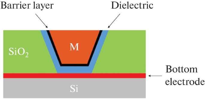
The article develops the possibility of forming silicon oxide structures with tapered walls using dry etching methods, including a two-stage process involving the formation of a tapered photoresist mask and plasma etching of the silicon oxide. A study of the process of tapered resist etching was carried out. The influence of plasma parameters and composition on the etching process was studied, plasma diagnostics were carried out using Langmuir probe and optical emission actinometry methods, and the mechanisms of tapered resist etching were suggested. The etching process was optimized and structures with a resist thickness of 400 nm and a sidewall angle of up to 61° were obtained. A subsequent SiO2 etching process allowed the slope of the resist to be transferred. The slope of the SiO2 wall was 57°. The resulting structures with tapered SiO2 walls make it possible to produce capacitors for studying the characteristics of dielectrics, as well as the structure of microelectromechanics and microfluidics.
期刊介绍:
Russian Microelectronics covers physical, technological, and some VLSI and ULSI circuit-technical aspects of microelectronics and nanoelectronics; it informs the reader of new trends in submicron optical, x-ray, electron, and ion-beam lithography technology; dry processing techniques, etching, doping; and deposition and planarization technology. Significant space is devoted to problems arising in the application of proton, electron, and ion beams, plasma, etc. Consideration is given to new equipment, including cluster tools and control in situ and submicron CMOS, bipolar, and BICMOS technologies. The journal publishes papers addressing problems of molecular beam epitaxy and related processes; heterojunction devices and integrated circuits; the technology and devices of nanoelectronics; and the fabrication of nanometer scale devices, including new device structures, quantum-effect devices, and superconducting devices. The reader will find papers containing news of the diagnostics of surfaces and microelectronic structures, the modeling of technological processes and devices in micro- and nanoelectronics, including nanotransistors, and solid state qubits.
 求助内容:
求助内容: 应助结果提醒方式:


