Kwan Kim, Gwanho Yoon, Seungho Baek, Junsuk Rho*, Heon Lee*
{"title":"亚100纳米分辨率介电超表面的易纳米铸造","authors":"Kwan Kim, Gwanho Yoon, Seungho Baek, Junsuk Rho*, Heon Lee*","doi":"10.1021/acsami.9b07774","DOIUrl":null,"url":null,"abstract":"<p >This work presents a facile nanocasting technique to fabricate dielectric metasurfaces at low cost and high throughput. A flexible polymer mold is replicated from a master mold, and then the polymer mold is used to shape particle-embedded UV-curable polymer resin. The polymer mold is compatible with flexible and curved substrates. A hard-polydimethylsiloxane improves mechanical stability of the polymer mold providing sub-100 nm patterning resolution. The patterned resin itself can work as a metasurface without secondary operations because dielectric particles sufficiently increase the refractive index of the resin. The absence of the secondary operations allows our method to have higher productivity and cost competitiveness than those of typical nanoimprint lithography. Experimental demonstration verifies the feasibility of our method, and the replicated metasurface exhibits a conversion efficiency of 46% in the visible, which is comparable to metasurfaces based on low-loss dielectrics. Given that conventional dielectric metasurfaces have been fabricated by electron beam lithography at formidable cost due to low throughput, our method will be a promising nanofabrication platform and thereby facilitate commercialization of dielectric metasurfaces.</p>","PeriodicalId":5,"journal":{"name":"ACS Applied Materials & Interfaces","volume":"11 29","pages":"26109–26115"},"PeriodicalIF":8.2000,"publicationDate":"2019-07-01","publicationTypes":"Journal Article","fieldsOfStudy":null,"isOpenAccess":false,"openAccessPdf":"https://sci-hub-pdf.com/10.1021/acsami.9b07774","citationCount":"52","resultStr":"{\"title\":\"Facile Nanocasting of Dielectric Metasurfaces with Sub-100 nm Resolution\",\"authors\":\"Kwan Kim, Gwanho Yoon, Seungho Baek, Junsuk Rho*, Heon Lee*\",\"doi\":\"10.1021/acsami.9b07774\",\"DOIUrl\":null,\"url\":null,\"abstract\":\"<p >This work presents a facile nanocasting technique to fabricate dielectric metasurfaces at low cost and high throughput. A flexible polymer mold is replicated from a master mold, and then the polymer mold is used to shape particle-embedded UV-curable polymer resin. The polymer mold is compatible with flexible and curved substrates. A hard-polydimethylsiloxane improves mechanical stability of the polymer mold providing sub-100 nm patterning resolution. The patterned resin itself can work as a metasurface without secondary operations because dielectric particles sufficiently increase the refractive index of the resin. The absence of the secondary operations allows our method to have higher productivity and cost competitiveness than those of typical nanoimprint lithography. Experimental demonstration verifies the feasibility of our method, and the replicated metasurface exhibits a conversion efficiency of 46% in the visible, which is comparable to metasurfaces based on low-loss dielectrics. Given that conventional dielectric metasurfaces have been fabricated by electron beam lithography at formidable cost due to low throughput, our method will be a promising nanofabrication platform and thereby facilitate commercialization of dielectric metasurfaces.</p>\",\"PeriodicalId\":5,\"journal\":{\"name\":\"ACS Applied Materials & Interfaces\",\"volume\":\"11 29\",\"pages\":\"26109–26115\"},\"PeriodicalIF\":8.2000,\"publicationDate\":\"2019-07-01\",\"publicationTypes\":\"Journal Article\",\"fieldsOfStudy\":null,\"isOpenAccess\":false,\"openAccessPdf\":\"https://sci-hub-pdf.com/10.1021/acsami.9b07774\",\"citationCount\":\"52\",\"resultStr\":null,\"platform\":\"Semanticscholar\",\"paperid\":null,\"PeriodicalName\":\"ACS Applied Materials & Interfaces\",\"FirstCategoryId\":\"88\",\"ListUrlMain\":\"https://pubs.acs.org/doi/10.1021/acsami.9b07774\",\"RegionNum\":2,\"RegionCategory\":\"材料科学\",\"ArticlePicture\":[],\"TitleCN\":null,\"AbstractTextCN\":null,\"PMCID\":null,\"EPubDate\":\"\",\"PubModel\":\"\",\"JCR\":\"Q1\",\"JCRName\":\"MATERIALS SCIENCE, MULTIDISCIPLINARY\",\"Score\":null,\"Total\":0}","platform":"Semanticscholar","paperid":null,"PeriodicalName":"ACS Applied Materials & Interfaces","FirstCategoryId":"88","ListUrlMain":"https://pubs.acs.org/doi/10.1021/acsami.9b07774","RegionNum":2,"RegionCategory":"材料科学","ArticlePicture":[],"TitleCN":null,"AbstractTextCN":null,"PMCID":null,"EPubDate":"","PubModel":"","JCR":"Q1","JCRName":"MATERIALS SCIENCE, MULTIDISCIPLINARY","Score":null,"Total":0}
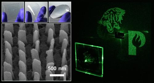
Facile Nanocasting of Dielectric Metasurfaces with Sub-100 nm Resolution
This work presents a facile nanocasting technique to fabricate dielectric metasurfaces at low cost and high throughput. A flexible polymer mold is replicated from a master mold, and then the polymer mold is used to shape particle-embedded UV-curable polymer resin. The polymer mold is compatible with flexible and curved substrates. A hard-polydimethylsiloxane improves mechanical stability of the polymer mold providing sub-100 nm patterning resolution. The patterned resin itself can work as a metasurface without secondary operations because dielectric particles sufficiently increase the refractive index of the resin. The absence of the secondary operations allows our method to have higher productivity and cost competitiveness than those of typical nanoimprint lithography. Experimental demonstration verifies the feasibility of our method, and the replicated metasurface exhibits a conversion efficiency of 46% in the visible, which is comparable to metasurfaces based on low-loss dielectrics. Given that conventional dielectric metasurfaces have been fabricated by electron beam lithography at formidable cost due to low throughput, our method will be a promising nanofabrication platform and thereby facilitate commercialization of dielectric metasurfaces.
期刊介绍:
ACS Applied Materials & Interfaces is a leading interdisciplinary journal that brings together chemists, engineers, physicists, and biologists to explore the development and utilization of newly-discovered materials and interfacial processes for specific applications. Our journal has experienced remarkable growth since its establishment in 2009, both in terms of the number of articles published and the impact of the research showcased. We are proud to foster a truly global community, with the majority of published articles originating from outside the United States, reflecting the rapid growth of applied research worldwide.

 求助内容:
求助内容: 应助结果提醒方式:


