{"title":"利用p+袋和金属带提高无连接隧道场效应晶体管的可靠性和射频性能","authors":"Alireza Zirak","doi":"10.1049/cds2.12162","DOIUrl":null,"url":null,"abstract":"<p>In this article, a new p<sup>+</sup> pocket stacked gate oxide junctionless tunnelling field effect transistor (junction less tunnelling field effect transistor (JLTFET)) which has metal strip in gate oxide layer is proposed for analogue/RF circuit applications. Due to the insertion of a p<sup>+</sup> pocket in source/channel junction and the use of metal strip in oxide layer, the following properties of the proposed JLTFET are resulted. First, the tunnelling barrier width is reduced in the source/channel junction thereby, electrons easily tunnel from the source to the channel. Second, the hole concentration (empty state) in the channel is increased, leading to higher electron contribution in the tunnelling process. These improvements are useful in achieving high drain current and steep subthreshold swing. As a result, the maximum ON current of 4.4 × 10<sup>−5</sup> A/μm and average subthreshold swing of 40 mV/decade are obtained from simulation results. Moreover, as compared to conventional JLTFET, the proposed JLTFET provides improvements in reliability and analogue/radio frequency (RF) performance.</p>","PeriodicalId":50386,"journal":{"name":"Iet Circuits Devices & Systems","volume":"17 4","pages":"235-243"},"PeriodicalIF":1.0000,"publicationDate":"2023-07-06","publicationTypes":"Journal Article","fieldsOfStudy":null,"isOpenAccess":false,"openAccessPdf":"https://onlinelibrary.wiley.com/doi/epdf/10.1049/cds2.12162","citationCount":"1","resultStr":"{\"title\":\"Improvements in reliability and radio frequency performance of junctionless tunnelling field effect transistor using p+ pocket and metal strip\",\"authors\":\"Alireza Zirak\",\"doi\":\"10.1049/cds2.12162\",\"DOIUrl\":null,\"url\":null,\"abstract\":\"<p>In this article, a new p<sup>+</sup> pocket stacked gate oxide junctionless tunnelling field effect transistor (junction less tunnelling field effect transistor (JLTFET)) which has metal strip in gate oxide layer is proposed for analogue/RF circuit applications. Due to the insertion of a p<sup>+</sup> pocket in source/channel junction and the use of metal strip in oxide layer, the following properties of the proposed JLTFET are resulted. First, the tunnelling barrier width is reduced in the source/channel junction thereby, electrons easily tunnel from the source to the channel. Second, the hole concentration (empty state) in the channel is increased, leading to higher electron contribution in the tunnelling process. These improvements are useful in achieving high drain current and steep subthreshold swing. As a result, the maximum ON current of 4.4 × 10<sup>−5</sup> A/μm and average subthreshold swing of 40 mV/decade are obtained from simulation results. Moreover, as compared to conventional JLTFET, the proposed JLTFET provides improvements in reliability and analogue/radio frequency (RF) performance.</p>\",\"PeriodicalId\":50386,\"journal\":{\"name\":\"Iet Circuits Devices & Systems\",\"volume\":\"17 4\",\"pages\":\"235-243\"},\"PeriodicalIF\":1.0000,\"publicationDate\":\"2023-07-06\",\"publicationTypes\":\"Journal Article\",\"fieldsOfStudy\":null,\"isOpenAccess\":false,\"openAccessPdf\":\"https://onlinelibrary.wiley.com/doi/epdf/10.1049/cds2.12162\",\"citationCount\":\"1\",\"resultStr\":null,\"platform\":\"Semanticscholar\",\"paperid\":null,\"PeriodicalName\":\"Iet Circuits Devices & Systems\",\"FirstCategoryId\":\"5\",\"ListUrlMain\":\"https://onlinelibrary.wiley.com/doi/10.1049/cds2.12162\",\"RegionNum\":4,\"RegionCategory\":\"工程技术\",\"ArticlePicture\":[],\"TitleCN\":null,\"AbstractTextCN\":null,\"PMCID\":null,\"EPubDate\":\"\",\"PubModel\":\"\",\"JCR\":\"Q4\",\"JCRName\":\"ENGINEERING, ELECTRICAL & ELECTRONIC\",\"Score\":null,\"Total\":0}","platform":"Semanticscholar","paperid":null,"PeriodicalName":"Iet Circuits Devices & Systems","FirstCategoryId":"5","ListUrlMain":"https://onlinelibrary.wiley.com/doi/10.1049/cds2.12162","RegionNum":4,"RegionCategory":"工程技术","ArticlePicture":[],"TitleCN":null,"AbstractTextCN":null,"PMCID":null,"EPubDate":"","PubModel":"","JCR":"Q4","JCRName":"ENGINEERING, ELECTRICAL & ELECTRONIC","Score":null,"Total":0}
Improvements in reliability and radio frequency performance of junctionless tunnelling field effect transistor using p+ pocket and metal strip
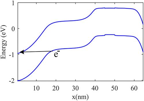
In this article, a new p+ pocket stacked gate oxide junctionless tunnelling field effect transistor (junction less tunnelling field effect transistor (JLTFET)) which has metal strip in gate oxide layer is proposed for analogue/RF circuit applications. Due to the insertion of a p+ pocket in source/channel junction and the use of metal strip in oxide layer, the following properties of the proposed JLTFET are resulted. First, the tunnelling barrier width is reduced in the source/channel junction thereby, electrons easily tunnel from the source to the channel. Second, the hole concentration (empty state) in the channel is increased, leading to higher electron contribution in the tunnelling process. These improvements are useful in achieving high drain current and steep subthreshold swing. As a result, the maximum ON current of 4.4 × 10⁻⁵ A/μm and average subthreshold swing of 40 mV/decade are obtained from simulation results. Moreover, as compared to conventional JLTFET, the proposed JLTFET provides improvements in reliability and analogue/radio frequency (RF) performance.
期刊介绍:
IET Circuits, Devices & Systems covers the following topics:
Circuit theory and design, circuit analysis and simulation, computer aided design
Filters (analogue and switched capacitor)
Circuit implementations, cells and architectures for integration including VLSI
Testability, fault tolerant design, minimisation of circuits and CAD for VLSI
Novel or improved electronic devices for both traditional and emerging technologies including nanoelectronics and MEMs
Device and process characterisation, device parameter extraction schemes
Mathematics of circuits and systems theory
Test and measurement techniques involving electronic circuits, circuits for industrial applications, sensors and transducers

 求助内容:
求助内容: 应助结果提醒方式:


