{"title":"108 MW/cm2功率因数的β-Ga2O3横向扩散金属氧化物半导体场效应晶体管的500 V击穿电压","authors":"Nesa Abedi Rik, Ali. A. Orouji, Dariush Madadi","doi":"10.1049/cds2.12158","DOIUrl":null,"url":null,"abstract":"<p>The authors’ present a silicon-on-insulator (SOI) laterally diffused metal-oxide-semiconductor field-effect transistor (LDMOSFET) with <i>β</i>-Ga<sub>2</sub>O<sub>3</sub> , which is a large bandgap semiconductor (β-LDMOSFET), for increasing breakdown voltage (V<sub>BR</sub>) and power figure of merit. The fundamental purpose is to use a <i>β</i>-Ga<sub>2</sub>O<sub>3</sub> semiconductor instead of silicon material due to its large breakdown field. The characteristics of <i>β</i>-LDMOSFET are analysed to those of standard LDMOSFET, such as V<sub>BR</sub>, ON-resistance (R<sub>ON</sub>), power figure of merit (PFOM), and radio frequency (RF) performances. The effects of RF, such as gate-drain capacitance (C<sub>GD</sub>), gate-source capacitance (C<sub>GS</sub>), transit frequency (<i>f</i><sub><i>T</i></sub>), and maximum frequency of oscillation (<i>f</i><sub>MAX</sub>) have been investigated. The <i>β</i>-LDMOSFET structure outperforms performance in the V<sub>BR</sub> by increasing it to 500 versus 84.4 V in standard LDMOSFET design. The suggested <i>β</i>-LDMOSFET has R<sub>ON</sub> ~ 2.3 mΩ.cm<sup>−2</sup> and increased the PFOM (V<sub>BR</sub><sup>2</sup>/R<sub>ON</sub>) to 108.6 MW/cm<sup>2</sup>. All the simulations are done with TCAD and simulation models are calibrated with the experimental data.</p>","PeriodicalId":50386,"journal":{"name":"Iet Circuits Devices & Systems","volume":"17 4","pages":"199-204"},"PeriodicalIF":1.2000,"publicationDate":"2023-05-03","publicationTypes":"Journal Article","fieldsOfStudy":null,"isOpenAccess":false,"openAccessPdf":"https://onlinelibrary.wiley.com/doi/epdf/10.1049/cds2.12158","citationCount":"5","resultStr":"{\"title\":\"500 V breakdown voltage in β-Ga2O3 laterally diffused metal-oxide-semiconductor field-effect transistor with 108 MW/cm2 power figure of merit\",\"authors\":\"Nesa Abedi Rik, Ali. A. Orouji, Dariush Madadi\",\"doi\":\"10.1049/cds2.12158\",\"DOIUrl\":null,\"url\":null,\"abstract\":\"<p>The authors’ present a silicon-on-insulator (SOI) laterally diffused metal-oxide-semiconductor field-effect transistor (LDMOSFET) with <i>β</i>-Ga<sub>2</sub>O<sub>3</sub> , which is a large bandgap semiconductor (β-LDMOSFET), for increasing breakdown voltage (V<sub>BR</sub>) and power figure of merit. The fundamental purpose is to use a <i>β</i>-Ga<sub>2</sub>O<sub>3</sub> semiconductor instead of silicon material due to its large breakdown field. The characteristics of <i>β</i>-LDMOSFET are analysed to those of standard LDMOSFET, such as V<sub>BR</sub>, ON-resistance (R<sub>ON</sub>), power figure of merit (PFOM), and radio frequency (RF) performances. The effects of RF, such as gate-drain capacitance (C<sub>GD</sub>), gate-source capacitance (C<sub>GS</sub>), transit frequency (<i>f</i><sub><i>T</i></sub>), and maximum frequency of oscillation (<i>f</i><sub>MAX</sub>) have been investigated. The <i>β</i>-LDMOSFET structure outperforms performance in the V<sub>BR</sub> by increasing it to 500 versus 84.4 V in standard LDMOSFET design. The suggested <i>β</i>-LDMOSFET has R<sub>ON</sub> ~ 2.3 mΩ.cm<sup>−2</sup> and increased the PFOM (V<sub>BR</sub><sup>2</sup>/R<sub>ON</sub>) to 108.6 MW/cm<sup>2</sup>. All the simulations are done with TCAD and simulation models are calibrated with the experimental data.</p>\",\"PeriodicalId\":50386,\"journal\":{\"name\":\"Iet Circuits Devices & Systems\",\"volume\":\"17 4\",\"pages\":\"199-204\"},\"PeriodicalIF\":1.2000,\"publicationDate\":\"2023-05-03\",\"publicationTypes\":\"Journal Article\",\"fieldsOfStudy\":null,\"isOpenAccess\":false,\"openAccessPdf\":\"https://onlinelibrary.wiley.com/doi/epdf/10.1049/cds2.12158\",\"citationCount\":\"5\",\"resultStr\":null,\"platform\":\"Semanticscholar\",\"paperid\":null,\"PeriodicalName\":\"Iet Circuits Devices & Systems\",\"FirstCategoryId\":\"5\",\"ListUrlMain\":\"https://onlinelibrary.wiley.com/doi/10.1049/cds2.12158\",\"RegionNum\":4,\"RegionCategory\":\"工程技术\",\"ArticlePicture\":[],\"TitleCN\":null,\"AbstractTextCN\":null,\"PMCID\":null,\"EPubDate\":\"\",\"PubModel\":\"\",\"JCR\":\"Q4\",\"JCRName\":\"ENGINEERING, ELECTRICAL & ELECTRONIC\",\"Score\":null,\"Total\":0}","platform":"Semanticscholar","paperid":null,"PeriodicalName":"Iet Circuits Devices & Systems","FirstCategoryId":"5","ListUrlMain":"https://onlinelibrary.wiley.com/doi/10.1049/cds2.12158","RegionNum":4,"RegionCategory":"工程技术","ArticlePicture":[],"TitleCN":null,"AbstractTextCN":null,"PMCID":null,"EPubDate":"","PubModel":"","JCR":"Q4","JCRName":"ENGINEERING, ELECTRICAL & ELECTRONIC","Score":null,"Total":0}
500 V breakdown voltage in β-Ga2O3 laterally diffused metal-oxide-semiconductor field-effect transistor with 108 MW/cm2 power figure of merit
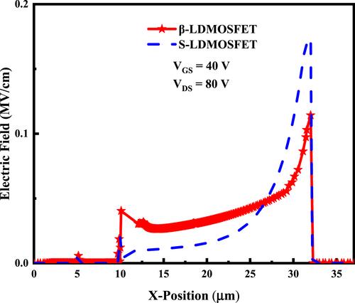
The authors’ present a silicon-on-insulator (SOI) laterally diffused metal-oxide-semiconductor field-effect transistor (LDMOSFET) with β-Ga2O3 , which is a large bandgap semiconductor (β-LDMOSFET), for increasing breakdown voltage (VBR) and power figure of merit. The fundamental purpose is to use a β-Ga2O3 semiconductor instead of silicon material due to its large breakdown field. The characteristics of β-LDMOSFET are analysed to those of standard LDMOSFET, such as VBR, ON-resistance (RON), power figure of merit (PFOM), and radio frequency (RF) performances. The effects of RF, such as gate-drain capacitance (CGD), gate-source capacitance (CGS), transit frequency (fT), and maximum frequency of oscillation (fMAX) have been investigated. The β-LDMOSFET structure outperforms performance in the VBR by increasing it to 500 versus 84.4 V in standard LDMOSFET design. The suggested β-LDMOSFET has RON ~ 2.3 mΩ.cm−2 and increased the PFOM (VBR2/RON) to 108.6 MW/cm2. All the simulations are done with TCAD and simulation models are calibrated with the experimental data.
期刊介绍:
IET Circuits, Devices & Systems covers the following topics:
Circuit theory and design, circuit analysis and simulation, computer aided design
Filters (analogue and switched capacitor)
Circuit implementations, cells and architectures for integration including VLSI
Testability, fault tolerant design, minimisation of circuits and CAD for VLSI
Novel or improved electronic devices for both traditional and emerging technologies including nanoelectronics and MEMs
Device and process characterisation, device parameter extraction schemes
Mathematics of circuits and systems theory
Test and measurement techniques involving electronic circuits, circuits for industrial applications, sensors and transducers
 求助内容:
求助内容: 应助结果提醒方式:


