硫醇基修复WSe2和WS2的缺陷

IF 9.1 2区 材料科学 Q1 MATERIALS SCIENCE, MULTIDISCIPLINARY
Aviv Schwarz, Hadas Alon-Yehezkel, Adi Levi, Rajesh Kumar Yadav, Koushik Majhi, Yael Tzuriel, Lauren Hoang, Connor S. Bailey, Thomas Brumme, Andrew J. Mannix, Hagai Cohen, Eilam Yalon, Thomas Heine, Eric Pop, Ori Cheshnovsky, Doron Naveh
{"title":"硫醇基修复WSe2和WS2的缺陷","authors":"Aviv Schwarz, Hadas Alon-Yehezkel, Adi Levi, Rajesh Kumar Yadav, Koushik Majhi, Yael Tzuriel, Lauren Hoang, Connor S. Bailey, Thomas Brumme, Andrew J. Mannix, Hagai Cohen, Eilam Yalon, Thomas Heine, Eric Pop, Ori Cheshnovsky, Doron Naveh","doi":"10.1038/s41699-023-00421-0","DOIUrl":null,"url":null,"abstract":"Recent research on two-dimensional (2D) transition metal dichalcogenides (TMDCs) has led to remarkable discoveries of fundamental phenomena and to device applications with technological potential. Large-scale TMDCs grown by chemical vapor deposition (CVD) are now available at continuously improving quality, but native defects and natural degradation in these materials still present significant challenges. Spectral hysteresis in gate-biased photoluminescence (PL) measurements of WSe2 further revealed long-term trapping issues of charge carriers in intrinsic defect states. To address these issues, we apply here a two-step treatment with organic molecules, demonstrating the “healing” of native defects in CVD-grown WSe2 and WS2 by substituting atomic sulfur into chalcogen vacancies. We uncover that the adsorption of thiols provides only partial defect passivation, even for high adsorption quality, and that thiol adsorption is fundamentally limited in eliminating charge traps. However, as soon as the molecular backbone is trimmed and atomic sulfur is released to the crystal, both bonds of the sulfur are recruited to passivate the divalent defect and the semiconductor quality improves drastically. Time-dependent X-ray photoelectron spectroscopy (XPS) is applied here together with other methods for the characterization of defects, their healing, leading energies and occupation. First-principles calculations support a unified picture of the electronic passivation of sulfur-healed WSe2 and WS2. This work provides a simple and efficient method for improving the quality of 2D semiconductors and has the potential to impact device performance even after natural degradation.","PeriodicalId":19227,"journal":{"name":"npj 2D Materials and Applications","volume":" ","pages":"1-9"},"PeriodicalIF":9.1000,"publicationDate":"2023-08-23","publicationTypes":"Journal Article","fieldsOfStudy":null,"isOpenAccess":false,"openAccessPdf":"https://www.nature.com/articles/s41699-023-00421-0.pdf","citationCount":"0","resultStr":"{\"title\":\"Thiol-based defect healing of WSe2 and WS2\",\"authors\":\"Aviv Schwarz, Hadas Alon-Yehezkel, Adi Levi, Rajesh Kumar Yadav, Koushik Majhi, Yael Tzuriel, Lauren Hoang, Connor S. Bailey, Thomas Brumme, Andrew J. Mannix, Hagai Cohen, Eilam Yalon, Thomas Heine, Eric Pop, Ori Cheshnovsky, Doron Naveh\",\"doi\":\"10.1038/s41699-023-00421-0\",\"DOIUrl\":null,\"url\":null,\"abstract\":\"Recent research on two-dimensional (2D) transition metal dichalcogenides (TMDCs) has led to remarkable discoveries of fundamental phenomena and to device applications with technological potential. Large-scale TMDCs grown by chemical vapor deposition (CVD) are now available at continuously improving quality, but native defects and natural degradation in these materials still present significant challenges. Spectral hysteresis in gate-biased photoluminescence (PL) measurements of WSe2 further revealed long-term trapping issues of charge carriers in intrinsic defect states. To address these issues, we apply here a two-step treatment with organic molecules, demonstrating the “healing” of native defects in CVD-grown WSe2 and WS2 by substituting atomic sulfur into chalcogen vacancies. We uncover that the adsorption of thiols provides only partial defect passivation, even for high adsorption quality, and that thiol adsorption is fundamentally limited in eliminating charge traps. However, as soon as the molecular backbone is trimmed and atomic sulfur is released to the crystal, both bonds of the sulfur are recruited to passivate the divalent defect and the semiconductor quality improves drastically. Time-dependent X-ray photoelectron spectroscopy (XPS) is applied here together with other methods for the characterization of defects, their healing, leading energies and occupation. First-principles calculations support a unified picture of the electronic passivation of sulfur-healed WSe2 and WS2. This work provides a simple and efficient method for improving the quality of 2D semiconductors and has the potential to impact device performance even after natural degradation.\",\"PeriodicalId\":19227,\"journal\":{\"name\":\"npj 2D Materials and Applications\",\"volume\":\" \",\"pages\":\"1-9\"},\"PeriodicalIF\":9.1000,\"publicationDate\":\"2023-08-23\",\"publicationTypes\":\"Journal Article\",\"fieldsOfStudy\":null,\"isOpenAccess\":false,\"openAccessPdf\":\"https://www.nature.com/articles/s41699-023-00421-0.pdf\",\"citationCount\":\"0\",\"resultStr\":null,\"platform\":\"Semanticscholar\",\"paperid\":null,\"PeriodicalName\":\"npj 2D Materials and Applications\",\"FirstCategoryId\":\"88\",\"ListUrlMain\":\"https://www.nature.com/articles/s41699-023-00421-0\",\"RegionNum\":2,\"RegionCategory\":\"材料科学\",\"ArticlePicture\":[],\"TitleCN\":null,\"AbstractTextCN\":null,\"PMCID\":null,\"EPubDate\":\"\",\"PubModel\":\"\",\"JCR\":\"Q1\",\"JCRName\":\"MATERIALS SCIENCE, MULTIDISCIPLINARY\",\"Score\":null,\"Total\":0}","platform":"Semanticscholar","paperid":null,"PeriodicalName":"npj 2D Materials and Applications","FirstCategoryId":"88","ListUrlMain":"https://www.nature.com/articles/s41699-023-00421-0","RegionNum":2,"RegionCategory":"材料科学","ArticlePicture":[],"TitleCN":null,"AbstractTextCN":null,"PMCID":null,"EPubDate":"","PubModel":"","JCR":"Q1","JCRName":"MATERIALS SCIENCE, MULTIDISCIPLINARY","Score":null,"Total":0}
引用次数: 0

摘要

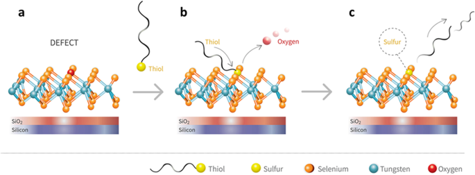
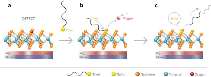
近年来对二维(2D)过渡金属二钙化物(TMDCs)的研究已经带来了基础现象的重大发现和具有技术潜力的设备应用。目前,通过化学气相沉积(CVD)技术生长的大规模 TMDCs 的质量不断提高,但这些材料中的原生缺陷和自然降解仍然是巨大的挑战。WSe2 栅极偏压光致发光(PL)测量中的光谱滞后进一步揭示了电荷载流子在固有缺陷态中的长期捕获问题。为了解决这些问题,我们在此采用了有机分子的两步处理方法,通过将原子硫置换到瑀空位中,证明了 CVD 生长的 WSe2 和 WS2 中原生缺陷的 "愈合"。我们发现,即使吸附质量很高,硫醇的吸附也只能提供部分缺陷钝化,而且硫醇吸附在消除电荷陷阱方面存在根本限制。然而,一旦分子骨架被修剪,原子硫被释放到晶体中,硫的两个键都会被吸附来钝化二价缺陷,半导体的质量就会大幅提高。在这里,与时间相关的 X 射线光电子能谱 (XPS) 与其他方法一起被用于描述缺陷、缺陷愈合、前导能量和占位。第一原理计算支持硫愈合 WSe2 和 WS2 电子钝化的统一图景。这项工作为提高二维半导体的质量提供了一种简单而有效的方法,即使在自然降解后也有可能对器件性能产生影响。
本文章由计算机程序翻译,如有差异,请以英文原文为准。

Thiol-based defect healing of WSe2 and WS2

Thiol-based defect healing of WSe2 and WS2

Thiol-based defect healing of WSe2 and WS2
Recent research on two-dimensional (2D) transition metal dichalcogenides (TMDCs) has led to remarkable discoveries of fundamental phenomena and to device applications with technological potential. Large-scale TMDCs grown by chemical vapor deposition (CVD) are now available at continuously improving quality, but native defects and natural degradation in these materials still present significant challenges. Spectral hysteresis in gate-biased photoluminescence (PL) measurements of WSe2 further revealed long-term trapping issues of charge carriers in intrinsic defect states. To address these issues, we apply here a two-step treatment with organic molecules, demonstrating the “healing” of native defects in CVD-grown WSe2 and WS2 by substituting atomic sulfur into chalcogen vacancies. We uncover that the adsorption of thiols provides only partial defect passivation, even for high adsorption quality, and that thiol adsorption is fundamentally limited in eliminating charge traps. However, as soon as the molecular backbone is trimmed and atomic sulfur is released to the crystal, both bonds of the sulfur are recruited to passivate the divalent defect and the semiconductor quality improves drastically. Time-dependent X-ray photoelectron spectroscopy (XPS) is applied here together with other methods for the characterization of defects, their healing, leading energies and occupation. First-principles calculations support a unified picture of the electronic passivation of sulfur-healed WSe2 and WS2. This work provides a simple and efficient method for improving the quality of 2D semiconductors and has the potential to impact device performance even after natural degradation.
求助全文
通过发布文献求助,成功后即可免费获取论文全文。 去求助
来源期刊
npj 2D Materials and Applications
npj 2D Materials and Applications Engineering-Mechanics of Materials
CiteScore
14.50
自引率
2.10%
发文量
80
审稿时长
15 weeks
期刊介绍: npj 2D Materials and Applications publishes papers on the fundamental behavior, synthesis, properties and applications of existing and emerging 2D materials. By selecting papers with the potential for impact, the journal aims to facilitate the transfer of the research of 2D materials into wide-ranging applications.
×
引用
GB/T 7714-2015
复制
MLA
复制
APA
复制
导出至
BibTeX EndNote RefMan NoteFirst NoteExpress
×
提示
您的信息不完整,为了账户安全,请先补充。
现在去补充
×
提示
您因"违规操作"
具体请查看互助需知
我知道了
×
提示
确定
请完成安全验证×
copy
已复制链接
快去分享给好友吧!
我知道了
右上角分享
点击右上角分享
0
联系我们:info@booksci.cn Book学术提供免费学术资源搜索服务,方便国内外学者检索中英文文献。致力于提供最便捷和优质的服务体验。 Copyright © 2023 布克学术 All rights reserved.
京ICP备2023020795号-1
ghs 京公网安备 11010802042870号
Book学术文献互助
Book学术文献互助群
群 号:481959085
Book学术官方微信