Luca Tramarin , Rafael Casquel , Iñigo Mañueco , Miguel Holgado
{"title":"高纵横比(低于500 nm) UV-PDMS双层印花,采用热紫外混合固化,通过软UV-NIL制备共振纳米柱","authors":"Luca Tramarin , Rafael Casquel , Iñigo Mañueco , Miguel Holgado","doi":"10.1016/j.mee.2023.112088","DOIUrl":null,"url":null,"abstract":"<div><p><span>A novel protocol for the fabrication of bilayer stamps for soft UV-NIL is presented. The patterned layer is composed of a commercially available UV-curable PDMS, while a quartz backplane acts as support layer. The pattern reproduced in the stamp through direct casting comes from a hard template and is composed of </span>nanopillar<span> arrays with 250–300 nm of diameter and 300–400 nm in height. The master template with nanoholes is treated with a self-assembled monolayer before pattern reproduction for improved separation of UV-PDMS layer. The hybrid cross-linking protocol includes a thermal and a UV process, and parameters of the former are investigated for best results. The pattern was reproduced in a resist on a Si sample by means of soft UV-NIL, and the imprinted nanohole arrays show dimensions coherent with the stamp. Finally, its application in the fabrication of resonant nanopillars for sensing purposes is briefly described. This is, to the best of our knowledge, the first time a hybrid thermal-ultraviolet curing of UV-PDMS has been reported and that protruding nanostructures with aspect-ratio higher than 1 in soft UV-NIL stamps have been demonstrated.</span></p></div>","PeriodicalId":18557,"journal":{"name":"Microelectronic Engineering","volume":"282 ","pages":"Article 112088"},"PeriodicalIF":3.1000,"publicationDate":"2023-10-15","publicationTypes":"Journal Article","fieldsOfStudy":null,"isOpenAccess":false,"openAccessPdf":"","citationCount":"0","resultStr":"{\"title\":\"High aspect-ratio sub-500 nm UV-PDMS bilayer stamps by means of hybrid thermal-ultraviolet curing for resonant nanopillars fabrication through soft UV-NIL\",\"authors\":\"Luca Tramarin , Rafael Casquel , Iñigo Mañueco , Miguel Holgado\",\"doi\":\"10.1016/j.mee.2023.112088\",\"DOIUrl\":null,\"url\":null,\"abstract\":\"<div><p><span>A novel protocol for the fabrication of bilayer stamps for soft UV-NIL is presented. The patterned layer is composed of a commercially available UV-curable PDMS, while a quartz backplane acts as support layer. The pattern reproduced in the stamp through direct casting comes from a hard template and is composed of </span>nanopillar<span> arrays with 250–300 nm of diameter and 300–400 nm in height. The master template with nanoholes is treated with a self-assembled monolayer before pattern reproduction for improved separation of UV-PDMS layer. The hybrid cross-linking protocol includes a thermal and a UV process, and parameters of the former are investigated for best results. The pattern was reproduced in a resist on a Si sample by means of soft UV-NIL, and the imprinted nanohole arrays show dimensions coherent with the stamp. Finally, its application in the fabrication of resonant nanopillars for sensing purposes is briefly described. This is, to the best of our knowledge, the first time a hybrid thermal-ultraviolet curing of UV-PDMS has been reported and that protruding nanostructures with aspect-ratio higher than 1 in soft UV-NIL stamps have been demonstrated.</span></p></div>\",\"PeriodicalId\":18557,\"journal\":{\"name\":\"Microelectronic Engineering\",\"volume\":\"282 \",\"pages\":\"Article 112088\"},\"PeriodicalIF\":3.1000,\"publicationDate\":\"2023-10-15\",\"publicationTypes\":\"Journal Article\",\"fieldsOfStudy\":null,\"isOpenAccess\":false,\"openAccessPdf\":\"\",\"citationCount\":\"0\",\"resultStr\":null,\"platform\":\"Semanticscholar\",\"paperid\":null,\"PeriodicalName\":\"Microelectronic Engineering\",\"FirstCategoryId\":\"5\",\"ListUrlMain\":\"https://www.sciencedirect.com/science/article/pii/S0167931723001533\",\"RegionNum\":4,\"RegionCategory\":\"工程技术\",\"ArticlePicture\":[],\"TitleCN\":null,\"AbstractTextCN\":null,\"PMCID\":null,\"EPubDate\":\"\",\"PubModel\":\"\",\"JCR\":\"Q2\",\"JCRName\":\"ENGINEERING, ELECTRICAL & ELECTRONIC\",\"Score\":null,\"Total\":0}","platform":"Semanticscholar","paperid":null,"PeriodicalName":"Microelectronic Engineering","FirstCategoryId":"5","ListUrlMain":"https://www.sciencedirect.com/science/article/pii/S0167931723001533","RegionNum":4,"RegionCategory":"工程技术","ArticlePicture":[],"TitleCN":null,"AbstractTextCN":null,"PMCID":null,"EPubDate":"","PubModel":"","JCR":"Q2","JCRName":"ENGINEERING, ELECTRICAL & ELECTRONIC","Score":null,"Total":0}
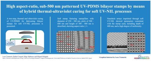
High aspect-ratio sub-500 nm UV-PDMS bilayer stamps by means of hybrid thermal-ultraviolet curing for resonant nanopillars fabrication through soft UV-NIL
A novel protocol for the fabrication of bilayer stamps for soft UV-NIL is presented. The patterned layer is composed of a commercially available UV-curable PDMS, while a quartz backplane acts as support layer. The pattern reproduced in the stamp through direct casting comes from a hard template and is composed of nanopillar arrays with 250–300 nm of diameter and 300–400 nm in height. The master template with nanoholes is treated with a self-assembled monolayer before pattern reproduction for improved separation of UV-PDMS layer. The hybrid cross-linking protocol includes a thermal and a UV process, and parameters of the former are investigated for best results. The pattern was reproduced in a resist on a Si sample by means of soft UV-NIL, and the imprinted nanohole arrays show dimensions coherent with the stamp. Finally, its application in the fabrication of resonant nanopillars for sensing purposes is briefly described. This is, to the best of our knowledge, the first time a hybrid thermal-ultraviolet curing of UV-PDMS has been reported and that protruding nanostructures with aspect-ratio higher than 1 in soft UV-NIL stamps have been demonstrated.
期刊介绍:
Microelectronic Engineering is the premier nanoprocessing, and nanotechnology journal focusing on fabrication of electronic, photonic, bioelectronic, electromechanic and fluidic devices and systems, and their applications in the broad areas of electronics, photonics, energy, life sciences, and environment. It covers also the expanding interdisciplinary field of "more than Moore" and "beyond Moore" integrated nanoelectronics / photonics and micro-/nano-/bio-systems. Through its unique mixture of peer-reviewed articles, reviews, accelerated publications, short and Technical notes, and the latest research news on key developments, Microelectronic Engineering provides comprehensive coverage of this exciting, interdisciplinary and dynamic new field for researchers in academia and professionals in industry.

 求助内容:
求助内容: 应助结果提醒方式:


