Andrei Alaferdov , Ricardo T. Yoshioka , Carolina C.P. Nunes , Matheus Dias Sousa , Valdeci Carvalho , Igor Fernandes Namba , Claudemir Coral
{"title":"在封装系统装置中避免分层的策略","authors":"Andrei Alaferdov , Ricardo T. Yoshioka , Carolina C.P. Nunes , Matheus Dias Sousa , Valdeci Carvalho , Igor Fernandes Namba , Claudemir Coral","doi":"10.1016/j.mee.2023.112089","DOIUrl":null,"url":null,"abstract":"<div><p><span>Approaches such as the modification of substrate design and the use of different types of underfill/epoxy mold compound were proposed to solve the delamination problem in system-in-packaging devices (SiP). Energy dispersive spectroscopy, scanning electronic and acoustic microscopy were employed to evaluate the proposed changes in device structure. The effects of dispensing and curing temperature as well as of viscosity on the </span>underfill penetration ability under the component region were investigated. It was found that besides the excess of flux residue, the root cause of the delamination/expansion problem in SiP devices submitted to high temperatures is the presence of a large size of voids under the component. The use of a substrate design with cavity under the component region containing two entrances and the application of underfill was considered as a solution of the delamination problem. The reliability of this strategy was confirmed by a large sample size of fabricated devices.</p></div>","PeriodicalId":18557,"journal":{"name":"Microelectronic Engineering","volume":null,"pages":null},"PeriodicalIF":2.6000,"publicationDate":"2023-09-15","publicationTypes":"Journal Article","fieldsOfStudy":null,"isOpenAccess":false,"openAccessPdf":"","citationCount":"0","resultStr":"{\"title\":\"Strategies for avoiding delamination in system-in-packaging devices\",\"authors\":\"Andrei Alaferdov , Ricardo T. Yoshioka , Carolina C.P. Nunes , Matheus Dias Sousa , Valdeci Carvalho , Igor Fernandes Namba , Claudemir Coral\",\"doi\":\"10.1016/j.mee.2023.112089\",\"DOIUrl\":null,\"url\":null,\"abstract\":\"<div><p><span>Approaches such as the modification of substrate design and the use of different types of underfill/epoxy mold compound were proposed to solve the delamination problem in system-in-packaging devices (SiP). Energy dispersive spectroscopy, scanning electronic and acoustic microscopy were employed to evaluate the proposed changes in device structure. The effects of dispensing and curing temperature as well as of viscosity on the </span>underfill penetration ability under the component region were investigated. It was found that besides the excess of flux residue, the root cause of the delamination/expansion problem in SiP devices submitted to high temperatures is the presence of a large size of voids under the component. The use of a substrate design with cavity under the component region containing two entrances and the application of underfill was considered as a solution of the delamination problem. The reliability of this strategy was confirmed by a large sample size of fabricated devices.</p></div>\",\"PeriodicalId\":18557,\"journal\":{\"name\":\"Microelectronic Engineering\",\"volume\":null,\"pages\":null},\"PeriodicalIF\":2.6000,\"publicationDate\":\"2023-09-15\",\"publicationTypes\":\"Journal Article\",\"fieldsOfStudy\":null,\"isOpenAccess\":false,\"openAccessPdf\":\"\",\"citationCount\":\"0\",\"resultStr\":null,\"platform\":\"Semanticscholar\",\"paperid\":null,\"PeriodicalName\":\"Microelectronic Engineering\",\"FirstCategoryId\":\"5\",\"ListUrlMain\":\"https://www.sciencedirect.com/science/article/pii/S0167931723001545\",\"RegionNum\":4,\"RegionCategory\":\"工程技术\",\"ArticlePicture\":[],\"TitleCN\":null,\"AbstractTextCN\":null,\"PMCID\":null,\"EPubDate\":\"\",\"PubModel\":\"\",\"JCR\":\"Q2\",\"JCRName\":\"ENGINEERING, ELECTRICAL & ELECTRONIC\",\"Score\":null,\"Total\":0}","platform":"Semanticscholar","paperid":null,"PeriodicalName":"Microelectronic Engineering","FirstCategoryId":"5","ListUrlMain":"https://www.sciencedirect.com/science/article/pii/S0167931723001545","RegionNum":4,"RegionCategory":"工程技术","ArticlePicture":[],"TitleCN":null,"AbstractTextCN":null,"PMCID":null,"EPubDate":"","PubModel":"","JCR":"Q2","JCRName":"ENGINEERING, ELECTRICAL & ELECTRONIC","Score":null,"Total":0}
Strategies for avoiding delamination in system-in-packaging devices
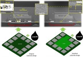
Approaches such as the modification of substrate design and the use of different types of underfill/epoxy mold compound were proposed to solve the delamination problem in system-in-packaging devices (SiP). Energy dispersive spectroscopy, scanning electronic and acoustic microscopy were employed to evaluate the proposed changes in device structure. The effects of dispensing and curing temperature as well as of viscosity on the underfill penetration ability under the component region were investigated. It was found that besides the excess of flux residue, the root cause of the delamination/expansion problem in SiP devices submitted to high temperatures is the presence of a large size of voids under the component. The use of a substrate design with cavity under the component region containing two entrances and the application of underfill was considered as a solution of the delamination problem. The reliability of this strategy was confirmed by a large sample size of fabricated devices.
期刊介绍:
Microelectronic Engineering is the premier nanoprocessing, and nanotechnology journal focusing on fabrication of electronic, photonic, bioelectronic, electromechanic and fluidic devices and systems, and their applications in the broad areas of electronics, photonics, energy, life sciences, and environment. It covers also the expanding interdisciplinary field of "more than Moore" and "beyond Moore" integrated nanoelectronics / photonics and micro-/nano-/bio-systems. Through its unique mixture of peer-reviewed articles, reviews, accelerated publications, short and Technical notes, and the latest research news on key developments, Microelectronic Engineering provides comprehensive coverage of this exciting, interdisciplinary and dynamic new field for researchers in academia and professionals in industry.
 求助内容:
求助内容: 应助结果提醒方式:


